Cinterion® EXSx2-W Hardware Interface Description Version: DocId: 01.200ee EXS62-W-EXS82-W_HID_v01.
Cinterion® EXS62-W/EXS82-W Hardware Interface Description Page 2 of 144 2 Document Name: Cinterion® EXS62-W/EXS82-W Hardware Interface Description Version: 01.200ee Date: 2022-09-07 DocId: EXS62-W-EXS82-W_HID_v01.200ee Status Public/ Released GENERAL NOTE THIS DOCUMENT CONTAINS INFORMATION ON THALES DIS AIS DEUTSCHLAND GMBH (“THALES”) PRODUCTS. THALES RESERVES THE RIGHT TO MAKE CHANGES TO THE PRODUCTS DESCRIBED HEREIN.
Cinterion® EXS62-W/EXS82-W Hardware Interface Description Page 3 of 144 Contents 144 Contents 1 Introduction ................................................................................................................. 9 1.1 Product Variants ................................................................................................ 9 1.2 Key Features at a Glance .................................................................................. 9 1.3 EXSx2-W System Overview .....................
Cinterion® EXS62-W/EXS82-W Hardware Interface Description Page 4 of 144 Contents 144 3.3 3.4 3.5 3.6 3.7 3.8 4 3.2.1.1 Switch on EXSx2-W Using ON Signal ................................ 63 3.2.1.2 Automatic Power On ........................................................... 65 3.2.2 Restart EXSx2-W................................................................................ 66 3.2.2.1 Restart EXSx2-W via AT+CFUN Command........................ 66 3.2.2.2 Restart EXSx2-W Using EMERG_RST............
Cinterion® EXS62-W/EXS82-W Hardware Interface Description Page 5 of 144 Contents 144 4.3 4.2.4.2 Processing Life...................................................................111 4.2.4.3 Baking ................................................................................111 4.2.4.4 Electrostatic Discharge ......................................................111 Packaging ...................................................................................................... 112 4.3.
Cinterion® EXS62-W/EXS82-W Hardware Interface Description Page 6 of 144 Tables 144 Tables Table 1: Table 2: Table 3: Table 4: Table 5: Table 6: Table 7: Table 8: Table 9: Table 10: Table 11: Table 12: Table 13: Table 14: Table 15: Table 16: Table 17: Table 18: Table 19: Table 20: Table 21: Table 22: Table 23: Table 24: Table 25: Table 26: Table 27: Table 28: Table 29: Table 30: Table 31: Table 32: Table 33: Table 34: Table 35: Table 36: na Table 37: 122 Table 38: Table 39: Table 40: Table 41: Table 42: T
Cinterion® EXS62-W/EXS82-W Hardware Interface Description Page 7 of 144 Figures 144 Figures Figure 1: Figure 2: Figure 3: Figure 4: Figure 5: Figure 6: Figure 7: Figure 8: Figure 9: Figure 10: Figure 11: Figure 12: Figure 13: Figure 14: Figure 15: Figure 16: Figure 17: Figure 18: Figure 19: Figure 20: Figure 21: Figure 22: Figure 23: Figure 24: Figure 25: Figure 26: Figure 27: Figure 28: Figure 29: Figure 30: Figure 31: Figure 32: Figure 33: Figure 34: Figure 35: Figure 36: Figure 37: Figure 38: Figure 3
Cinterion® EXS62-W/EXS82-W Hardware Interface Description Page 8 of 144 Figures 144 Figure 48: Figure 49: Figure 50: Figure 51: Figure 52: Figure 53: Figure 54: Figure 55: Figure 56: Figure 57: Figure 58: Figure 59: Figure 60: Figure 61: Figure 62: Figure 63: Figure 64: Figure 65: Figure 66: Figure 67: Figure 68: Figure 69: Figure 70: Figure 71: t Position of reference points BATT+ and GND ............................................... 96 ESD protection for RF antenna interface .......................
Cinterion® EXS62-W/EXS82-W Hardware Interface Description Page 9 of 144 1 Introduction 15 1 Introduction This document1 describes the hardware of the Cinterion® EXSx2-W module variants optimized for global coverage as they support a comprehensive set of bands required for global deployment. It helps you quickly retrieve interface specifications, electrical and mechanical details and information on the requirements to be considered for integrating further components. 1.
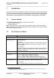
Cinterion® EXS62-W/EXS82-W Hardware Interface Description Page 10 of 144 1.2 Key Features at a Glance 15 Feature Implementation Power supply (see Section 2.1.2, and --> Section 3.4) Normal range: EXS82-W: - LTE and GSM: 3.3V to 4.6V - LTE with GSM deactivated: 2.8V to 4.6V EXS62-W ResM: - LTE: 2.8V to 4.6V Extended range: :EXS82-W - LTE with GSM deactivated: 2.5V to 4.8V EXS62-W ResM: - LTE: 2.5V to 4.8V Operating temperature (board temperature) (see Section 3.
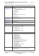
Cinterion® EXS62-W/EXS82-W Hardware Interface Description Page 11 of 144 1.2 Key Features at a Glance 15 Feature Implementation GNSS Features Modes (see Section 2.3) Standalone GNSS (GPS, GLONASS, BeiDou, Galileo) Protocol NMEA (for GNSS related sentences) General Automatic power saving modes Software AT commands Hayes 3GPP TS 27.007, TS 27.005, Thales AT commands for RIL compatibility Embedded processing platform (optional) Embedded processing option with API.
Cinterion® EXS62-W/EXS82-W Hardware Interface Description Page 12 of 144 1.2 Key Features at a Glance 15 Feature Implementation ADC input Analog-to-Digital Converter with one unbalanced analog input. SIM switch (see Section 2.1.11.4) Supports signal to switch between two externally connected SIMs. Antenna interface pads (see Section 2.2) 50Ω. GSM/LTE Main antenna, GNSS antenna I2C interface (see Section 2.1.9) I2C interface only available with embedded processing option.
Cinterion® EXS62-W/EXS82-W Hardware Interface Description Page 13 of 144 1.3 EXSx2-W System Overview 15 1.
Cinterion® EXS62-W/EXS82-W Hardware Interface Description Page 14 of 144 1.4 Circuit Concept 15 1.4 Circuit Concept Figure 3 and Figure 3 show block diagrams for the EXSx2-W module variants, and illustrate the major functional components: LGA Pads Antenna LGA Pads BATT+_RF Power Supply GPIO HWID’s BATT+ EN IN RF Part USB_VDDA _3P3 REFE 1...2_ CLK_DATA SDR_ TX_LB_GSM SDR_ TX_ MB_ GSM SDR_ ASM _AN T USIM CCIN 3 2 GSMPA +ASM Serial (ASC0) Serial (ASC1/GPIO) USB 2.
Cinterion® EXS62-W/EXS82-W Hardware Interface Description Page 15 of 144 1.4 Circuit Concept 15 LGA Pads Power Supply GPIO HWID’s BATT+ Antenna LGA Pads EN IN RF Part Coupler USB_VDDA _3P3 GPIO’s 8 4 3 Serial (ASC0) Serial (ASC1/GPIO) USB 2.0 3 USIM CCIN REFE 1...
Cinterion® EXS62-W/EXS82-W Hardware Interface Description Page 16 of 144 2 Interface Characteristics 61 2 Interface Characteristics EXSx2-W is equipped with an SMT application interface that connects to the external application. The SMT application interface incorporates the various application interfaces as well as the RF antenna interface. 2.1 Application Interface 2.1.
Cinterion® EXS62-W/EXS82-W Hardware Interface Description Page 17 of 144 2.1 Application Interface 61 Table 1: Overview: Pad assignments1 2 Pad no.
Cinterion® EXS62-W/EXS82-W Hardware Interface Description Page 18 of 144 2.
Cinterion® EXS62-W/EXS82-W Hardware Interface Description Page 19 of 144 2.
Cinterion® EXS62-W/EXS82-W Hardware Interface Description Page 20 of 144 2.1 Application Interface 61 2.1.2 Signal Properties Table 2: Signal properties Function Signal name IO Signal form and level Comment Power supply BATT+BB I Voltage ranges: Lines of BATT+ and GND must be connected in parallel for supply purposes because higher peak currents may occur. LTE and GSM (EXS82-W only): VImin = 3.3 V...VImax = 4.6V LTE with GSM deactivated VImin = 2.8 V...VImax = 4.
Cinterion® EXS62-W/EXS82-W Hardware Interface Description Page 21 of 144 2.1 Application Interface 61 Table 2: Signal properties Function Signal name IO Signal form and level Comment External supply voltage V180 O Normal operation: VOnorm = 1.80V ±2% IOmax = 10mA V180 has to be used for the power indication circuit. SLEEP mode Operation: VOSleep = 1.80V ±3.7% IOmax = 10mA V180 can also be used to supply level shifters at the interfaces.
Cinterion® EXS62-W/EXS82-W Hardware Interface Description Page 22 of 144 2.1 Application Interface 61 Table 2: Signal properties Function Signal name IO Signal form and level Comment USB VUSB_IN I VImin = 3V VImax = 5.25V All electrical characteristics according to USB Implementers' Forum, USB 2.0 Specification. Active and suspend current: Imax < 100µA USB_DN Serial Modem Interface ASC0 Serial Modem Interface ASC1 If unused keep lines open.
Cinterion® EXS62-W/EXS82-W Hardware Interface Description Page 23 of 144 2.1 Application Interface 61 Table 2: Signal properties Function Signal name IO Signal form and level Comment 1.8V eUICC interface CC2_VPP -- Used for single wire protocol (SWP NFC) in MFF-XS eUICC. SWP NFC is currently not supported and deactivated for the eUICC.
Cinterion® EXS62-W/EXS82-W Hardware Interface Description Page 24 of 144 2.1 Application Interface 61 Table 2: Signal properties Function 2 IC Signal name IO I2CDAT I/O Internal pull up Resistors I2CCLK = 2k2 O I2CDAT = 2k2 I2CCLK Signal form and level VOLmax = 0.45V at Imax = -4.5mA VOHmax = 1.95V VILmax = 0.5V VIHmin = 1.3V VIHmax = 1.95V Comment If unused keep lines open. Compatible with I2C Bus Specification Version 5.
Cinterion® EXS62-W/EXS82-W Hardware Interface Description Page 25 of 144 2.1 Application Interface 61 2.1.2.1 Absolute Maximum Ratings The absolute maximum ratings stated in Table 3 are stress ratings under any conditions. Stresses beyond any of these limits will cause permanent damage to EXSx2-W. Table 3: Absolute maximum ratings Parameter Min Max Unit Supply voltage BATT+BB (no service) -0.5 +6.0 V Supply voltage BATT+RF (EXS82-W only; no service) -0.5 +6.0 V -0.5 +0.5 V -0.3 +2.
Cinterion® EXS62-W/EXS82-W Hardware Interface Description Page 26 of 144 2.1 Application Interface 61 2.1.3 USB Interface EXSx2-W supports a USB 2.0 High Speed (480Mbit/s) device interface that is Full Speed (12Mbit/s) compliant. The external application is responsible for supplying the VUSB_IN line. This line is used for cable detection only. The USB part (driver and transceiver) is supplied by means of BATT+.
Cinterion® EXS62-W/EXS82-W Hardware Interface Description Page 27 of 144 2.1 Application Interface 61 2.1.4 Serial Interface ASC0 EXSx2-W offers an 8-wire unbalanced, asynchronous modem interface ASC0 conforming to ITU-T V.24 protocol DCE signaling. The electrical characteristics do not comply with ITU-T V.28. The significant levels are 0V (for low data bit or active state) and 1.8V (for high data bit or inactive state). For electrical characteristics please refer to Table 2.
Cinterion® EXS62-W/EXS82-W Hardware Interface Description Page 28 of 144 2.1 Application Interface 61 The following figure shows the startup behavior of the asynchronous serial interface ASC0.
Cinterion® EXS62-W/EXS82-W Hardware Interface Description Page 29 of 144 2.1 Application Interface 61 2.1.5 Serial Interface ASC1 EXSx2-W provides a 4-wire unbalanced, asynchronous modem interface ASC1 conforming to ITU-T V.24 protocol DCE signaling. The electrical characteristics do not comply with ITU-T V.28. The significant levels are 0V (for low data bit or active state) and 1.8V (for high data bit or inactive state). For electrical characteristics please refer to Table 2.
Cinterion® EXS62-W/EXS82-W Hardware Interface Description Page 30 of 144 2.1 Application Interface 61 The following figure shows the startup behavior of the asynchronous serial interface ASC1. Power supply active Start up Reset state Firmware initialization Command interface initialization Interface active ON VCORE V180 EMERG_RST TXD1 PD RXD1 PD RTS1 PD CTS1 PD PD PD Dotted lines indicate possible alternative signal states - depending on externally provided signal states.
Cinterion® EXS62-W/EXS82-W Hardware Interface Description Page 31 of 144 2.1 Application Interface 61 2.1.6 UICC/SIM/USIM Interface EXSx2-W has an integrated UICC/SIM/USIM interface compatible with the 3GPP 31.102 and ETSI 102 221. This is wired to the host interface in order to be connected to an external SIM card holder. Five pads on the SMT application interface are reserved for the SIM interface. The UICC/SIM/USIM interface supports 1.8V SIM cards.
Cinterion® EXS62-W/EXS82-W Hardware Interface Description Page 32 of 144 2.1 Application Interface 61 The figure below shows a circuit to connect an external SIM card holder.
Cinterion® EXS62-W/EXS82-W Hardware Interface Description Page 33 of 144 2.1 Application Interface 61 2.1.6.1 Enhanced ESD Protection for SIM Interface To optimize ESD protection for the SIM interface it is possible to add ESD diodes (e.g., NUP4114) to the SIM interface lines as shown in the example given in Figure 12. The example was designed to meet ESD protection according ETSI EN 301 489-1/7: Contact discharge: ± 4kV, air discharge: ± 8kV.
Cinterion® EXS62-W/EXS82-W Hardware Interface Description Page 34 of 144 2.1 Application Interface 61 2.1.7 eUICC Interface As an option EXSx2-W supports an eUICC in MFF-XS format. This MFF-XS eUICC is located under the shielding, is only connected to specific module pads, and has no physical connections with other circuits inside the module.
Cinterion® EXS62-W/EXS82-W Hardware Interface Description Page 35 of 144 2.1 Application Interface 61 If using a SIM switch to change between usage of an external SIM and an eUICC as shown in Figure 13, the module needs to be prepared for this dual mode by AT command. By default, dual mode is disabled, and usage of the first SIM slot, i.e.
Cinterion® EXS62-W/EXS82-W Hardware Interface Description Page 36 of 144 2.1 Application Interface 61 In case the module is mounted onto the LGA DevKit, a direct connection to the eUICC can be achieved by bridging the following pads on the backside of the LGA DevKit: PAD 249 to 17, PAD 248 to 19, PAD 247 to 21, PAD 246 to 20, as also shown in Figure 15. Figure 15: Interface bridging t EXS62-W_EXS82-W_HID_v01.
Cinterion® EXS62-W/EXS82-W Hardware Interface Description Page 37 of 144 2.1 Application Interface 61 2.1.8 GPIO Interface EXSx2-W has 7GPIOs for external hardware devices. Each GPIO can be configured for use as input or output. All settings are AT command controlled. The configuration is non-volatile and available after module restart. The IO port driver has to be opened before using and configuring GPIOs. Before changing the configuration of a GPIO pin (e.g. input to output) the pin has to be closed.
Cinterion® EXS62-W/EXS82-W Hardware Interface Description Page 38 of 144 2.1 Application Interface 61 2.1.8.1 GPIOs Available with Embedded Processing Option The embedded processing option of EXSx2-W provides a GPIO interface with 13 configurable GPIO lines. Some GPIO lines are shared with other interfaces or functions, and are shown in the following table with their default assignments being marked green.
Cinterion® EXS62-W/EXS82-W Hardware Interface Description Page 39 of 144 2.1 Application Interface 61 2.1.9 I2C Interface The embedded processing option of EXSx2-W provides an inter-integrated circuit interface. I2C is a serial, 8-bit oriented data transfer bus for bit rates up to 400kbps in Fast mode. It consists of two lines, the serial data line I2CDAT and the serial clock line I2CCLK. The module acts as a single master device, e.g. the clock I2CCLK is driven by the module.
Cinterion® EXS62-W/EXS82-W Hardware Interface Description Page 40 of 144 2.1 Application Interface 61 2.1.10 SPI Interface The embedded processing option of EXSx2-W provides an SPI interface where four GPIO interface lines can be configured as Serial Peripheral Interface (SPI). The SPI is a synchronous serial interface allowing the module to control external sensors or components. The SPI interface supports only master mode. The transmission rates are up to 6.5Mbit/s.
Cinterion® EXS62-W/EXS82-W Hardware Interface Description Page 41 of 144 2.1 Application Interface 61 2.1.11 2.1.11.1 Control Signals Status LED The STATUS line can be configured to drive a status LED that indicates different operating modes of the module. For details on how to configure status signaling please refer to [1]. To take advantage of this function connect an LED to the STATUS line as shown in Figure 19. The sample circuit is not optimized for low current consumption.
Cinterion® EXS62-W/EXS82-W Hardware Interface Description Page 42 of 144 2.1 Application Interface 61 10k External power supply Power indication 22k 100k V180 Figure 20: Power indication circuit 2.1.11.3 Fast Shutdown The FST_SHDN line triggers the module’s fast shutdown procedure. The fast shutdown procedure ensures data integrity during shutdown, but will no longer deregister gracefully from the network thus saving the time normally required for network deregistration.
Cinterion® EXS62-W/EXS82-W Hardware Interface Description Page 43 of 144 2.1 Application Interface 61 T0 T1 T2 T3 For timing values see Table 7. BATT+BB High V180 High Low VCORE High Low FST_SHDN High Low Figure 21: Fast shutdown timing Table 7: Fast shutdown timing values Timing Description Value Unit T0 – T1 FST_SHDN - V180 14.95 ms T1 – T2 V180 - V180 (low) 1.57 T2 – T3 V180 (low) - VCORE 1.
Cinterion® EXS62-W/EXS82-W Hardware Interface Description Page 44 of 144 2.1 Application Interface 61 Note: Vmax can be limited by the module supply and/or capacitor voltage. Same applies for the Vmin which is mostly limited by VBATT min. Module energy usage: Vavg = Vmax + Vmin / 2 Aavg = See typical values in Section 3.4.1 E[W] = Vavg * Aavg * Efficiency Example: Power Circuit Efficiency factor, e.g = 0.8 E[W] = ((4.5V + 3.0V) / 2) * 0.2A * 0.8 = 0.
Cinterion® EXS62-W/EXS82-W Hardware Interface Description Page 45 of 144 2.1 Application Interface 61 2.1.11.4 SIM Switch The UICC/USIM/SIM interface lines may be connected to an external SIM card multiplexer controlled by the SIM_SWITCH signal as shown in Figure 22. Thus, it becomes possible to switch between two networks/subscriptions each with their own UICC, and maybe different connection speeds. Please note that hot SIM insert/removal is only possible on the first SIM interface.
Cinterion® EXS62-W/EXS82-W Hardware Interface Description Page 46 of 144 2.2 RF Antenna Interface 61 2.2 RF Antenna Interface The RF interface has an impedance of 50Ω. EXSx2-W is capable of sustaining a total mismatch at the antenna line without any damage, even when transmitting at maximum RF power. The external antenna must be matched properly to achieve best performance regarding radiated power, modulation accuracy and harmonic suppression.
Cinterion® EXS62-W/EXS82-W Hardware Interface Description Page 47 of 144 2.2 RF Antenna Interface 61 Table 9: RF Antenna interface GSM / LTE1 Parameter Conditions Min.
Cinterion® EXS62-W/EXS82-W Hardware Interface Description Page 48 of 144 2.2 RF Antenna Interface 61 Table 9: RF Antenna interface GSM / LTE1 Parameter Conditions Min.2 Typical Unit LTE Cat NB1/2: Power @ ARP with 50Ω Load, NTNV Configuration ID: 1, UL: Modulation: BPSK; Subcarrier: 1;Subcarrier space: 3.
Cinterion® EXS62-W/EXS82-W Hardware Interface Description Page 49 of 144 2.2 RF Antenna Interface 61 Table 9: RF Antenna interface GSM / LTE1 Parameter Conditions GSM 850/900 RF Power @ ARP with 50Ω Load, (ROPR = 6) Min.2 Typical Unit GPRS, 1 TX 32.5 dBm GPRS, 2 TX 30.5 dBm EDGE, 1 TX 27.0 dBm EDGE, 2TX 27.0 dBm GSM 1800/1900 GPRS, 1 TX 29.5 dBm GPRS, 2 TX 27.5 dBm EDGE, 1 TX 26.0 dBm EDGE, 2TX 26.0 dBm GPRS, 1 TX 32.5 dBm GPRS, 2 TX 29.5 dBm EDGE, 1 TX 27.
Cinterion® EXS62-W/EXS82-W Hardware Interface Description Page 50 of 144 2.2 RF Antenna Interface 61 2.2.2 Antenna Installation The antennas is connected by soldering the antenna pads (RF_OUT, ANT_GNSS) and its neighboring ground pads directly to the application’s PCB.
Cinterion® EXS62-W/EXS82-W Hardware Interface Description Page 51 of 144 2.2 RF Antenna Interface 61 2.2.3 2.2.3.1 RF Line Routing Design Line Arrangement Examples Several dedicated tools are available to calculate line arrangements for specific applications and PCB materials - for example from http://www.polarinstruments.com/ (commercial software) or from https://www.awr.com/software/options/tx-line (free software).
Cinterion® EXS62-W/EXS82-W Hardware Interface Description Page 52 of 144 2.2 RF Antenna Interface 61 Micro-Stripline This section gives two line arrangement examples for micro-stripline. • Micro-Stripline on 1.0mm Standard FR4 2-Layer PCB The following two figures show examples with different values for D1 (ground strip separation). Application board Ground line Antenna line Ground line Figure 25: Micro-Stripline on 1.0mm standard FR4 2-layer PCB - example 1 t EXS62-W_EXS82-W_HID_v01.
Cinterion® EXS62-W/EXS82-W Hardware Interface Description Page 53 of 144 2.2 RF Antenna Interface 61 Application board Ground line Antenna line Ground line Figure 26: Micro-Stripline on 1.0mm Standard FR4 PCB - example 2 t EXS62-W_EXS82-W_HID_v01.
Cinterion® EXS62-W/EXS82-W Hardware Interface Description Page 54 of 144 2.2 RF Antenna Interface 61 • Micro-Stripline on 1.5mm Standard FR4 2-Layer PCB The following two figures show examples with different values for D1 (ground strip separation). Application board Ground line Antenna line Ground line Figure 27: Micro-Stripline on 1.5mm Standard FR4 PCB - example 1 t EXS62-W_EXS82-W_HID_v01.
Cinterion® EXS62-W/EXS82-W Hardware Interface Description Page 55 of 144 2.2 RF Antenna Interface 61 Application board Ground line Antenna line Ground line Figure 28: Micro-Stripline on 1.5mm Standard FR4 PCB - example 2 t EXS62-W_EXS82-W_HID_v01.
Cinterion® EXS62-W/EXS82-W Hardware Interface Description Page 56 of 144 2.2 RF Antenna Interface 61 2.2.3.2 Routing Example Interface to RF Connector Figure 29 shows the connection of the module‘s antenna pad with an application PCB‘s coaxial antenna connector. Please note that the EXSx2-W bottom plane appears mirrored, since it is viewed from EXSx2-W top side. By definition the top of customer's board shall mate with the bottom of the EXSx2-W module.
Cinterion® EXS62-W/EXS82-W Hardware Interface Description Page 57 of 144 2.3 GNSS Interface 61 2.3 GNSS Interface 2.3.1 GNSS Receiver EXSx2-W integrates a GNSS receiver that offers the full performance of GPS/GLONASS/BeiDou/Galileo technology. The GNSS receiver is able to continuously track all satellites in view, thus providing accurate satellite position data. The integrated GNSS receiver supports the NMEA protocol.
Cinterion® EXS62-W/EXS82-W Hardware Interface Description Page 58 of 144 2.3 GNSS Interface 61 2.3.3 GNSS Antenna Interface Characteristics Table 10: GNSS properties Parameter Conditions Horizontal accuracy 50% CEP, open sky Min. Maximal update rate Frequency Tracking Sensitivity Acquisition Sensitivity Time-to-First-Fix (TTFF)1 Typical Max. Unit 2 m 1 Hz GPS 1573.397 1575.420 1576.443 MHz GLONASS 1598.563 1602.563 1606.563 Beidou 1559.052 1561.098 1563.144 Galileo 1573.397 1575.
Cinterion® EXS62-W/EXS82-W Hardware Interface Description Page 59 of 144 2.4 Sample Application 61 2.4 Sample Application Figure 31 shows a typical example of how to integrate a EXSx2-W module with an application. Usage of the various host interfaces depends on the desired features of the application. Note that the sample application is not optimized for low current consumption.
Cinterion® EXS62-W/EXS82-W Hardware Interface Description Page 60 of 144 2.4 Sample Application 61 For switch on circuit see Section 3.2.1 BATT+BB EXSx2-W 150K Main antenna GND RF_OUT 22K ESD ** GND ON GND 10K ANT_GNSS GNSS antenna ESD ** GND RF * EMERG_RST 100K BATT+RF RF * BATT+BB V180 Power indication 33pF 150µF, Low ESR! 0K 22K 100K 47µF, Low ESR! 33pF Power supply Low ESR!, e.g., X7 R MLCC VCORE Blocking**** Blocking**** Blocking**** 5 4 8 3 GPIO20...
Cinterion® EXS62-W/EXS82-W Hardware Interface Description Page 61 of 144 2.4 Sample Application 61 2.4.1 Sample Level Conversion Circuit Depending on the micro controller used by an external application EXSx2-W‘s digital input and output lines (i.e., ASC0, ASC1) may require level conversion. The following Figure 32 shows a sample circuit with recommended level shifters for an external application‘s micro controller (with VLOGIC between 3.0V...3.6V).
Cinterion® EXS62-W/EXS82-W Hardware Interface Description Page 62 of 144 3 Operating Characteristics 102 3 Operating Characteristics 3.1 Operating Modes The table below briefly summarizes the various operating modes referred to throughout the document. Table 11: Overview of operating modes Mode Function Normal operation Data transfer GSM/(E)GPRS/LTE M1 NB1/2 data transfer in progress.
Cinterion® EXS62-W/EXS82-W Hardware Interface Description Page 63 of 144 3.2 Power Up/Power Down Scenarios 102 3.2 Power Up/Power Down Scenarios Do not turn on EXSx2-W while it is beyond the safety limits of voltage stated in Section 2.1.2.1. EXSx2-W immediately switches off after having started and detected these inappropriate conditions. In extreme cases this can cause permanent damage to the module. 3.2.
Cinterion® EXS62-W/EXS82-W Hardware Interface Description Page 64 of 144 3.2 Power Up/Power Down Scenarios 102 T0 T1 T2 T3 T4 T5 For timing values see Table 12.
Cinterion® EXS62-W/EXS82-W Hardware Interface Description Page 65 of 144 3.2 Power Up/Power Down Scenarios 102 Note: During the boot up phase of the module, the fast shutdown functionality, i.e., the use of the FST_SHDN line as described in Section 2.1.11.3, is not available. The FST_SHDN functionality becomes active only at T5 (see Table 12). In case of a power loss before the FST_SHDN line is active (T5), the data integrity is ensured even without the FST_SHDN functionality.
Cinterion® EXS62-W/EXS82-W Hardware Interface Description Page 66 of 144 3.2 Power Up/Power Down Scenarios 102 3.2.2 Restart EXSx2-W After startup EXSx2-W can be re-started as described in the following sections: • Software controlled reset by AT+CFUN command: Starts Normal mode (see Section 3.2.2.1). • Hardware controlled reset by EMERG_RST line: Starts Normal mode (see Section 3.2.2.2) 3.2.2.1 Restart EXSx2-W via AT+CFUN Command To reset and restart the EXSx2-W module use the command AT+CFUN.
Cinterion® EXS62-W/EXS82-W Hardware Interface Description Page 67 of 144 3.2 Power Up/Power Down Scenarios 102 Table 13: EMERG_RST restart timing values Timing Description Value Unit T0 - T1 EMERG_RST - V180 785.79 ms T1 - T2 V180 – V180 (low) 1.55 T2 - T3 V180 (low) – VCORE 1.66 It is strongly recommended to control this EMERG_RST line with an open collector transistor or an open drain field-effect transistor.
Cinterion® EXS62-W/EXS82-W Hardware Interface Description Page 68 of 144 3.2 Power Up/Power Down Scenarios 102 3.2.3 Signal States after Startup Table 14 describes various states interface signals pass through after startup until the system is active. Signals are in an initial state while the module is initializing. Once the startup initialization has completed, i.e. when the software is running, all signals are in a defined state, the module is ready to receive and transmit data.
Cinterion® EXS62-W/EXS82-W Hardware Interface Description Page 69 of 144 3.2 Power Up/Power Down Scenarios 102 3.2.4 Turn off EXSx2-W To switch the module off the following procedures may be used: • Software controlled shutdown procedure: Software controlled by sending an AT command over the serial application interface. See Section 3.2.4.1. • Hardware controlled shutdown procedure: Hardware controlled by setting the FST_SHDN line to low. See Section 2.1.11.3.
Cinterion® EXS62-W/EXS82-W Hardware Interface Description Page 70 of 144 3.2 Power Up/Power Down Scenarios 102 Table 15: Switch off timing values (AT^SMSO) Timing Description Value Unit 1 T0 - T1 AT^SMSO – URC 247.15 (depending on network) T1 - T2 URC – V180 14.19 T2 - T3 V180 – V180 (low) 1.53 T3 - T4 V180 (low) – VCORE 1.64 ms 1. Value is dependent on network, and may take up to 5 seconds for LTE Cat NB1/2 networks.
Cinterion® EXS62-W/EXS82-W Hardware Interface Description Page 71 of 144 3.2 Power Up/Power Down Scenarios 102 3.2.5 Automatic Shutdown Automatic shutdown takes effect if the following event occurs: • The EXSx2-W board is exceeding the critical limits of overtemperature or undertemperature (see Section 3.2.5.1) • Undervoltage or overvoltage is detected (see Section 3.2.5.2 and Section 3.2.5.3) The automatic shutdown procedure is equivalent to the power-down initiated with an AT command, i.e.
Cinterion® EXS62-W/EXS82-W Hardware Interface Description Page 72 of 144 3.2 Power Up/Power Down Scenarios 102 3.2.5.2 Undervoltage Shutdown The undervoltage shutdown threshold is the specified minimum supply voltage VBATT+ given in Table 21. When the average supply voltage measured by EXSx2-W approaches the undervoltage shutdown threshold (i.e., 0.
Cinterion® EXS62-W/EXS82-W Hardware Interface Description Page 73 of 144 3.3 Power Saving 102 3.3 Power Saving EXSx2-W can control its power consumption through specific features as summarized in Table 18, and further detailed in the following sections. The mentioned operating modes are detailed in Section 3.1. For typical power supply ratings during power saving please refer to Section 3.4.1.
Cinterion® EXS62-W/EXS82-W Hardware Interface Description Page 74 of 144 3.3 Power Saving 102 3.3.1 Low Power Modes There are two specific low power modes available that can be configured to allow EXSx2-W to save power - SLEEP mode (Section 3.3.1.1) and SUSPEND mode (Section 3.3.1.2). Figure 38 illustrates how the module transits between its operating modes including SLEEP and SUSPEND modes.
Cinterion® EXS62-W/EXS82-W Hardware Interface Description Page 75 of 144 3.3 Power Saving 102 3.3.1.1 SLEEP Mode SLEEP mode is a module’s low power mode when no call is in progress and there is no active communication on any serial interface (ASC0, ASC1). During SLEEP mode, the serial interfaces are shut down except for RTS0 that may be used to wake up EXSx2-W from SLEEP mode (see below).
Cinterion® EXS62-W/EXS82-W Hardware Interface Description Page 76 of 144 3.3 Power Saving 102 3.3.1.2 SUSPEND Mode In contrast to SLEEP mode, SUSPEND mode is a module’s low power mode with almost all components switched off - except for the internal RTC and interrupt triggered wake up mechanisms. The module stays registered to the network, and the RRC connection is released. The module is in its lowest power consumption state.
Cinterion® EXS62-W/EXS82-W Hardware Interface Description Page 77 of 144 3.3 Power Saving 102 From SUSPEND mode the module can only be woken up by the ON or EMERG_RST signals, or it may wake up and be reachable again after expiration of a negotiated 3GPP PSM periodic TAU cycle (i.e., network timer) that may include DRX as well as eDRX paging cycles for an inactivity period (see Section 3.3.3.3 for details).
Cinterion® EXS62-W/EXS82-W Hardware Interface Description Page 78 of 144 3.3 Power Saving 102 3.3.2 Power Saving while Attached to GSM Networks (EXS82-W only) Power saving while attached to GSM networks is based on standard DRX values defined for the network (see Section 3.3.2.1). Apart from network based power saving it is possible to use the AT command AT^SCFG="Radio/OutputPowerReduction" for the module in (E)GPRS multislot scenarios to reduce its output power according to 3GPP 45.005.
Cinterion® EXS62-W/EXS82-W Hardware Interface Description Page 79 of 144 3.3 Power Saving 102 3.3.3 Power Saving while Attached to LTE M1 NB1/2 Networks This section describes the power saving possibilities in LTE Cat M1 and LTE Cat NB1/2 networks through DRX (see Section 3.3.3.1) values, as well as configurable eDRX (see Section 3.3.3.2), and 3GPP PSM (see Section 3.3.3.3) timers. 3.3.3.
Cinterion® EXS62-W/EXS82-W Hardware Interface Description Page 80 of 144 3.3 Power Saving 102 3.3.3.2 eDRX (Extended DRX Configuration) EXSx2-W and the network may negotiate the use of eDRX (extended DRX) to reduce power consumption, while being available for mobile terminating data and/or network originated procedures within a certain delay dependent on the network negotiated eDRX cycle value (see also Section 3.3.1.2).
Cinterion® EXS62-W/EXS82-W Hardware Interface Description Page 81 of 144 3.3 Power Saving 102 3.3.3.3 3GPP PSM Configuration EXSx2-W can be configured to use 3GPP PSM to reduce power consumption. PSM is similar to power off, while EXSx2-W remains registered with the network. There is no need to re-attach or re-establish PDN connections. EXSx2-W in PSM is not immediately reachable for mobile terminating services (see also SUSPEND mode in Section 3.3.1.2).
Cinterion® EXS62-W/EXS82-W Hardware Interface Description Page 82 of 144 3.4 Power Supply 102 3.4 Power Supply EXSx2-W needs to be connected to a power supply at the SMT application interface - 2 lines BATT+, and GND. There are two separate voltage domains for BATT+: • BATT+BB with a line mainly for the baseband power supply. • BATT+RF with a line for the GSM power amplifier supply. Please note that this line needs only be connected for GSM (2G/3G) availability.
Cinterion® EXS62-W/EXS82-W Hardware Interface Description Page 83 of 144 3.4 Power Supply 102 Table 20: General current consumption ratings (EXSx2-W) Description IBATT+ Conditions Typical rating 1 OFF State POWER DOWN supply cur(i.e., sum of rent BATT+BB Airplane UART (RTS) active and 2 mode BATT+RF ) (CFUN = 4) UART (RTS) inactive Unit EXS62-W EXS82-W 14 14.7 µA 8.29 8.07 mA 0.71 0.74 mA 1. With an impedance of ZLOAD=50Ω at the antenna connector, Measured at 25°C at 3.8V. 2.
Cinterion® EXS62-W/EXS82-W Hardware Interface Description Page 84 of 144 3.4 Power Supply 102 Table 21: Current consumption ratings Cat M1 (EXSx2-W) Description IBATT+ 1 (i.e.
Cinterion® EXS62-W/EXS82-W Hardware Interface Description Page 85 of 144 3.4 Power Supply 102 Table 21: Current consumption ratings Cat M1 (EXSx2-W) Description IBATT+ 1 (i.e., only BATT+BB ) t Conditions Typical rating Unit EXS62-W EXS82-W Peak Current @ RRC con- Band1, 20dBm nected Active Transmission3 Band2, 20dBm VBATT = 3.
Cinterion® EXS62-W/EXS82-W Hardware Interface Description Page 86 of 144 3.4 Power Supply 102 Table 21: Current consumption ratings Cat M1 (EXSx2-W) Description IBATT+ 1 (i.e., only BATT+BB ) Conditions Average idle supply current (GNSS on) Typical rating Unit EXS62-W EXS82-W CAT-M1 active (UART active) @ DRX=128 GNSS NMEA output off 68 67 mA GPRS active (UART active) @ DRX=128 GNSS NMEA output on 68 65 mA 1. With an impedance of ZLOAD=50Ω at the antenna connector, Measured at 25°C at 3.
Cinterion® EXS62-W/EXS82-W Hardware Interface Description Page 87 of 144 3.4 Power Supply 102 Table 22: Current consumption ratings Cat NB1/2 (EXSx2-W) Description IBATT+ 1 (i.e., only BATT+BB ) Conditions SUSPEND Average LTE NB1/2 RRC idle supply (SLEEP)2 current 2 RRC idle (SUSPEND)2 t Typical rating Unit EXS62-W EXS82-W Power save mode 3.3 4.3 µA DRX=1024 0.91 1.05 mA DRX=512 1.18 1.37 mA DRX=256 1.01 1.16 mA DRX=128 1.42 1.57 mA 20,48s eDRX 2,56s paging window (DRX=1.
Cinterion® EXS62-W/EXS82-W Hardware Interface Description Page 88 of 144 3.4 Power Supply 102 Table 22: Current consumption ratings Cat NB1/2 (EXSx2-W) Description IBATT+ 1 (i.e.
Cinterion® EXS62-W/EXS82-W Hardware Interface Description Page 89 of 144 3.4 Power Supply 102 Table 22: Current consumption ratings Cat NB1/2 (EXSx2-W) Description IBATT+ 1 (i.e.
Cinterion® EXS62-W/EXS82-W Hardware Interface Description Page 90 of 144 3.4 Power Supply 102 Table 22: Current consumption ratings Cat NB1/2 (EXSx2-W) Description IBATT+ 1 (i.e.
Cinterion® EXS62-W/EXS82-W Hardware Interface Description Page 91 of 144 3.4 Power Supply 102 Table 22: Current consumption ratings Cat NB1/2 (EXSx2-W) Description IBATT+ 1 (i.e., only BATT+BB ) t Conditions Typical rating Unit EXS62-W EXS82-W Peak Current @ RRC connected Band1, 20dBm Active Transmission UL RMC, Band2, 20dBm single tone mode (1subcar3 rier),15KHz spacing Band3, 20dBm VBATT=3.
Cinterion® EXS62-W/EXS82-W Hardware Interface Description Page 92 of 144 3.4 Power Supply 102 Table 22: Current consumption ratings Cat NB1/2 (EXSx2-W) Description IBATT+ 1 (i.e., only BATT+BB ) Conditions Typical rating Unit EXS62-W EXS82-W Peak Current @ RRC connected Band1, 20dBm Active Transmission UL RMC, Band2, 20dBm single tone mode (1subcar3 rier),15KHz spacing Band3, 20dBm VBATT =2.
Cinterion® EXS62-W/EXS82-W Hardware Interface Description Page 93 of 144 3.4 Power Supply 102 Table 23: Current consumption GSM (EXS82-W only) Description IBATT+1 (i.e., only BATT+BB ) Conditions Typical rating Unit 0.94 mA 1.20 mA 1.94 mA SLEEP @DRX=2, UART (RTS) active 9 mA GPRS Data transfer GSM850; PCL=5,1Tx/4RX ROPR=8 (max. reduction) 246 mA ROPR=4 (no reduction) 248 mA ROPR=8 (max. reduction) 346 mA ROPR=4 (no reduction) 445 mA ROPR=8 (max.
Cinterion® EXS62-W/EXS82-W Hardware Interface Description Page 94 of 144 3.4 Power Supply 102 Table 23: Current consumption GSM (EXS82-W only) Description IBATT+1 (i.e., only BATT+BB ) Conditions Unit Average GSM GPRS Data transfer GSM1800; supply current PCL=0; 2Tx/3Rx (GPS off) ROPR=8 (max. reduction) 275 mA ROPR=4 (no reduction) 341 mA EDGE Data transfer GSM1800; PCL=0; 1Tx/4Rx ROPR=8 (max. reduction) 152 mA ROPR=4 (no reduction) 154 mA ROPR=8 (max.
Cinterion® EXS62-W/EXS82-W Hardware Interface Description Page 95 of 144 3.4 Power Supply 102 Table 23: Current consumption GSM (EXS82-W only) Description IBATT+1 (i.e., only BATT+BB ) Conditions Average GPRS active (UART active) @ DRX=2 GSM idle sup- GNSS NMEA output off ply current GPRS active (UART active) @ DRX=2 (GNSS on) GNSS NMEA output on Typical rating Unit 64 mA 68 mA 1. With an impedance of ZLOAD=50Ω at the antenna connector, Measured at 25°C at 3.8V. 2.
Cinterion® EXS62-W/EXS82-W Hardware Interface Description Page 96 of 144 3.4 Power Supply 102 3.4.2 Minimizing Power Losses For EXS62-W ResM only: When designing the power supply for your application (and with GSM enabled) please pay specific attention to power losses. Ensure that the input voltage VBATT+ never drops below 3.3V on the EXSx2-W board, not even in a GSM transmit burst where current consumption can rise (for peak values see the power supply ratings listed in Section 3.4.1).
Cinterion® EXS62-W/EXS82-W Hardware Interface Description Page 97 of 144 3.4 Power Supply 102 3.4.4 Monitoring Power Supply by AT Command To monitor the supply voltage you can also use the AT^SBV command which returns the value related to the reference points BATT+ and GND. The module continuously measures the voltage at intervals depending on the operating mode of the RF interface. The duration of measuring ranges from 0.
Cinterion® EXS62-W/EXS82-W Hardware Interface Description Page 98 of 144 3.5 Operating Temperatures 102 3.5 Operating Temperatures Please note that the module’s lifetime, i.e., the MTTF (mean time to failure) may be reduced, if operated outside the extended temperature range. Table 24: Board temperature Parameter Min Max Unit -30 +85 °C Extended operation -40 +90 °C Automatic shutdown2 Temperature measured on EXSx2-W board <-40 >+90 °C Normal operation 1 Typ --- 1.
Cinterion® EXS62-W/EXS82-W Hardware Interface Description Page 99 of 144 3.6 Electrostatic Discharge 102 3.6 Electrostatic Discharge The GSM module is not protected against Electrostatic Discharge (ESD) in general. Consequently, it is subject to ESD handling precautions that typically apply to ESD sensitive components. Proper ESD handling and packaging procedures must be applied throughout the processing, handling and operation of any application that incorporates a EXSx2-W module.
Cinterion® EXS62-W/EXS82-W Hardware Interface Description Page 100 of 144 3.7 Blocking against RF on Interface Lines 102 3.7 Blocking against RF on Interface Lines To reduce EMI issues there are serial resistors, or capacitors to GND, implemented on the module for the ignition, emergency restart, and SIM interface lines (cp. Section 2.4). However, all other signal lines have no EMI measures on the module and there are no blocking measures at the module’s interface to an external application.
Cinterion® EXS62-W/EXS82-W Hardware Interface Description Page 101 of 144 3.7 Blocking against RF on Interface Lines 102 The following table lists for each signal line at the module‘s SMT application interface the EMI measures that may be implemented. Table 27: EMI measures on the application interface Signal name EMI measures A B C CCIN Remark D E x CCRST x The external capacitor should be not higher than 1nF.
Cinterion® EXS62-W/EXS82-W Hardware Interface Description Page 102 of 144 3.8 Reliability Characteristics 102 3.8 Reliability Characteristics The test conditions stated below are an extract of the complete test specifications.
Cinterion® EXS62-W/EXS82-W Hardware Interface Description Page 103 of 144 4 Mechanical Dimensions, Mounting and Packaging 119 4 Mechanical Dimensions, Mounting and Packaging 4.1 Mechanical Dimensions of EXSx2-W Figure 51 shows the top and bottom view of EXSx2-W and provides an overview of the board's mechanical dimensions. For further details see Figure 52. Figure 53 shows the area at the module’s bottom side where possible markings might be printed.
Cinterion® EXS62-W/EXS82-W Hardware Interface Description Page 104 of 144 4.1 Mechanical Dimensions of EXSx2-W 119 Figure 52: Dimensions of EXSx2-W (all dimensions in mm) Area for markings at center of module’s PCB: 13mm x 5mm Figure 53: Dimensions of area for possible markings (bottom view) t EXS62-W_EXS82-W_HID_v01.
Cinterion® EXS62-W/EXS82-W Hardware Interface Description Page 105 of 144 4.2 Mounting EXSx2-W onto the Application Platform 119 4.2 Mounting EXSx2-W onto the Application Platform This section describes how to mount EXSx2-W onto the PCBs, including land pattern and stencil design, board-level characterization, soldering conditions, durability and mechanical handling. For more information on issues related to SMT module integration see also [5].
Cinterion® EXS62-W/EXS82-W Hardware Interface Description Page 106 of 144 4.2 Mounting EXSx2-W onto the Application Platform 119 The stencil design illustrated in Figure 55 and Figure 56 is recommended by Thales as a result of extensive tests with Thales Daisy Chain modules. The central ground pads are primarily intended for stabilizing purposes, and may show some more voids than the application interface pads at the module's rim. This is acceptable, since they are electrically irrelevant.
Cinterion® EXS62-W/EXS82-W Hardware Interface Description Page 107 of 144 4.2 Mounting EXSx2-W onto the Application Platform 119 4.2.1.2 Board Level Characterization Board level characterization issues should also be taken into account if devising an SMT process. Characterization tests should attempt to optimize the SMT process with regard to board level reliability.
Cinterion® EXS62-W/EXS82-W Hardware Interface Description Page 108 of 144 4.2 Mounting EXSx2-W onto the Application Platform 119 4.2.3 Soldering Conditions and Temperature 4.2.3.1 Reflow Profile tP TP TL tL TSmax Temperature TSmin tS Preheat t to maximum Time Figure 57: Reflow Profile t EXS62-W_EXS82-W_HID_v01.
Cinterion® EXS62-W/EXS82-W Hardware Interface Description Page 109 of 144 4.2 Mounting EXSx2-W onto the Application Platform 119 Table 29: Reflow temperature ratings1 Profile Feature Pb-Free Assembly Preheat & Soak Temperature Minimum (TSmin) Temperature Maximum (TSmax) Time (tSmin to tSmax) (tS) 150°C 180°C 60-120 seconds Average ramp up rate (TSmax to TP) 3K/second max.
Cinterion® EXS62-W/EXS82-W Hardware Interface Description Page 110 of 144 4.2 Mounting EXSx2-W onto the Application Platform 119 4.2.4 Durability and Mechanical Handling 4.2.4.1 Storage Conditions EXSx2-W modules, as delivered in tape and reel carriers, must be stored in sealed, moisture barrier anti-static bags. The conditions stated below are only valid for modules in their original packed state in weather protected, non-temperature-controlled storage locations.
Cinterion® EXS62-W/EXS82-W Hardware Interface Description Page 111 of 144 4.2 Mounting EXSx2-W onto the Application Platform 119 4.2.4.2 Processing Life EXSx2-W must be soldered to an application within 72 hours after opening the moisture barrier bag (MBB) it was stored in. As specified in the IPC/JEDEC J-STD-033 Standard, the manufacturing site processing the modules should have ambient temperatures below 30°C and a relative humidity below 60%. 4.2.4.
Cinterion® EXS62-W/EXS82-W Hardware Interface Description Page 112 of 144 4.3 Packaging 119 4.3 Packaging 4.3.1 Tape and Reel The single-feed tape carrier for EXSx2-W is illustrated in Figure 58. The figure also shows the proper part orientation. The tape width is 44mm and the EXSx2-W modules are placed on the tape with a 32-mm pitch. The reels are 330mm in diameter with a core diameter of 100mm. Each reel contains 500 modules. 4.3.1.
Cinterion® EXS62-W/EXS82-W Hardware Interface Description Page 113 of 144 4.3 Packaging 119 4.3.1.2 Barcode Label A barcode label provides detailed information on the tape and its contents. It is attached to the reel. Barcode label Figure 60: Barcode label on tape reel Figure 61: Barcode label on tape reel - layout Variables on the label are explained in Table 31. t EXS62-W_EXS82-W_HID_v01.
Cinterion® EXS62-W/EXS82-W Hardware Interface Description Page 114 of 144 4.3 Packaging 119 4.3.2 Shipping Materials EXSx2-W is distributed in tape and reel carriers. The tape and reel carriers used to distribute EXSx2-W are packed as described below, including the following required shipping materials: • Moisture barrier bag, including desiccant and humidity indicator card • Transportation box 4.3.2.
Cinterion® EXS62-W/EXS82-W Hardware Interface Description Page 115 of 144 4.3 Packaging 119 Figure 63: Moisture Sensitivity Label t EXS62-W_EXS82-W_HID_v01.
Cinterion® EXS62-W/EXS82-W Hardware Interface Description Page 116 of 144 4.3 Packaging 119 MBBs contain one or more desiccant pouches to absorb moisture that may be in the bag. The humidity indicator card described below should be used to determine whether the enclosed components have absorbed an excessive amount of moisture. The desiccant pouches should not be baked or reused once removed from the MBB.
Cinterion® EXS62-W/EXS82-W Hardware Interface Description Page 117 of 144 4.3 Packaging 119 4.3.2.2 Transportation Box Tape and reel carriers are distributed in a box, marked with a barcode label for identification purposes. A box contains two reels with 500 modules each. 1 2 3 4 5 8 6 9 7 10 11 12 14 13 Figure 65: Sample of VP box label Table 31: VP Box label information No.
Cinterion® EXS62-W/EXS82-W Hardware Interface Description Page 118 of 144 4.3 Packaging 119 4.3.3 Trays If small module quantities are required, e.g., for test and evaluation purposes, EXSx2-W may be distributed in trays (for dimensions see Figure 69). The small quantity trays are an alternative to the single-feed tape carriers normally used. However, the trays are not designed for machine processing.
Cinterion® EXS62-W/EXS82-W Hardware Interface Description Page 119 of 144 4.3 Packaging 119 Figure 69: Tray dimensions t EXS62-W_EXS82-W_HID_v01.
Cinterion® EXS62-W/EXS82-W Hardware Interface Description Page 120 of 144 5 Regulatory and Type Approval Information 128 5 Regulatory and Type Approval Information 5.1 Directives and Standards EXSx2-W is designed to comply with the directives and standards listed below.
Cinterion® EXS62-W/EXS82-W Hardware Interface Description Page 121 of 144 5.1 Directives and Standards 128 Table 34: Standards of European type approval 3GPP TS 51.010-1 Digital cellular telecommunications system (Release 7); Mobile Station (MS) conformance specification; GCF-CC V3.71 Global Certification Forum - Certification Criteria ETSI EN 301 511 V12.5.
Cinterion® EXS62-W/EXS82-W Hardware Interface Description Page 122 of 144 5.1 Directives and Standards 128 Table 36: Standards of the Ministry of Information Industry of the People’s Republic of China SJ/T 11363-2006 “Requirements for Concentration Limits for Certain Hazardous Substances in Electronic Information Products” (2006-06). SJ/T 11364-2006 “Marking for Control of Pollution Caused by Electronic Information Products” (2006-06).
Cinterion® EXS62-W/EXS82-W Hardware Interface Description Page 123 of 144 5.1 Directives and Standards 128 5.1.1 IEC 62368-1 Classification With respect to the safety requirements for audio/video, information and communication technology equipment defined by the hazard based product safety standard for ICT and AV equipment - i.e., IEC-62368-1 (EN 62368-1, UL 62368-1) - Cinterion® modules are classified as shown below: Standalone operation of the modules is not possible.
Cinterion® EXS62-W/EXS82-W Hardware Interface Description Page 124 of 144 5.1 Directives and Standards 128 Table 38: IEC 62368-1 Classification Source of Energy Class Limits Hazardous Substances, Chemical reaction -- Under regular conditions, the Cinterion® module does not contain any chemically reactive substances, and no chemical energy source, especially no battery. Module is compliant with RoHS and REACH (see above). In very rare cases however - under abnormal conditions (i.e.
Cinterion® EXS62-W/EXS82-W Hardware Interface Description Page 125 of 144 5.2 SAR requirements specific to portable mobiles 128 5.2 SAR requirements specific to portable mobiles Mobile phones, PDAs or other portable transmitters and receivers incorporating a GSM module must be in accordance with the guidelines for human exposure to radio frequency energy.
Cinterion® EXS62-W/EXS82-W Hardware Interface Description Page 126 of 144 5.3 Reference Equipment for Type Approval 128 5.
Cinterion® EXS62-W/EXS82-W Hardware Interface Description Page 129 of 144 6 Document Information 140 6 Document Information 6.1 Revision History Preceding document: "Cinterion® EXS62-W/EXS82-W Hardware Interface Description" v01.200e New document: "Cinterion® EXS62-W/EXS82-W Hardware Interface Description" v01.200ee Chapter What is new 2.1 Table 2 Fast Shutdown section update. 3.2.4 Caution note added. 5.4 Table 39 updated with band 85 information.
Cinterion® EXS62-W/EXS82-W Hardware Interface Description Page 130 of 144 6.1 Revision History 140 7.1 Revised ordering information for EXS62-W Evaluation Module. 7.2 Updated module label information. Preceding document: "Cinterion® EXS62-W/EXS82-W Hardware Interface Description" v01.200 New document: "Cinterion® EXS62-W/EXS82-W Hardware Interface Description" v01.200a Chapter What is new 2.1.2, 3.2.1.1 Revised high level pulse width for ON signal (1ms --> 30ms). 3.2.1.
Cinterion® EXS62-W/EXS82-W Hardware Interface Description Page 131 of 144 6.1 Revision History 140 Chapter What is new 2.1.2 Detailed description for EMERG_RST signal in Table 2. 2.4 Replaced “PWR_IND” with “Power indication” in Figure 31. Preceding document: "Cinterion® EXS62-W/EXS82-W Hardware Interface Description" v01.100b New document: "Cinterion® EXS62-W/EXS82-W Hardware Interface Description"v01.100c Chapter What is new 3.4.1 Updated power supply ratings. 7.
Cinterion® EXS62-W/EXS82-W Hardware Interface Description Page 132 of 144 6.1 Revision History 140 New document: "Cinterion® EXS62-W/EXS82-W Hardware Interface Description" v01.003 Chapter What is new Throughout document Added support for MIM (MFF2 UICC) interface. 1.2 Added support for Cinterion® IoT Module services (MODS) as key feature. 2.1.7 New section eUICC Interface. 3.4.1 Revised power supply ratings. 3.6 Added CDM to table showing electrostatic values.
Cinterion® EXS62-W/EXS82-W Hardware Interface Description Page 133 of 144 6.1 Revision History 140 Chapter What is new 4.2.1.1 Replaced land pattern and stencil figures. 4.3.1.2 Added Figure 61 with sample bar code label layout. 4.3.2.2 Added Figure 65 and Table 31 with VP box label information. 7.2 New section Module Label Information. Preceding document: "Cinterion® EXS62-W/EXS82-W Hardware Interface Description" v00.
Cinterion® EXS62-W/EXS82-W Hardware Interface Description Page 134 of 144 6.1 Revision History 140 Chapter What is new 2.1.1 Revised representation of pad layout. Preceding document: "Cinterion® EXS62-W/EXS82-W Hardware Interface Description" v00.005 New document: "Cinterion® EXS62-W/EXS82-W Hardware Interface Description" v00.011 Chapter What is new 1.2 Revised table listing key features. 2.1.2 Revised Table 2 listing signal properties. 2.1.2.
Cinterion® EXS62-W/EXS82-W Hardware Interface Description Page 135 of 144 6.1 Revision History 140 Throughout document Added EXS62-W as supported product variant. Added 300bps as lowest baud rate supported by ASC0 and ASC1. Removed support for LTE Cat M1 Bd71, as well as LTE Cat NB1/2 Bd17 and Bd71. 1.4 Updated Figure 2 and Figure 3 with block diagrams. 5.4 Replaced “IC” with “ISED”. New document: "Cinterion® EXS82-W Hardware Interface Description" Version 00.001 v01.
Cinterion® EXS62-W/EXS82-W Hardware Interface Description Page 136 of 144 6.2 Related Documents 140 6.2 [1] [2] [3] [4] [5] [6] [7] [8] [9] [10] Related Documents EXSx2-W AT Command Set EXSx2-W Release Note Universal Serial Bus Specification Revision 2.
Cinterion® EXS62-W/EXS82-W Hardware Interface Description Page 137 of 144 6.
Cinterion® EXS62-W/EXS82-W Hardware Interface Description Page 138 of 144 6.
Cinterion® EXS62-W/EXS82-W Hardware Interface Description Page 139 of 144 6.3 Terms and Abbreviations 140 Abbreviation Description TE Terminal Equipment, also referred to as DTE TLS Transport Layer Security Tx Transmit Direction UART Universal asynchronous receiver-transmitter URC Unsolicited Result Code USSD Unstructured Supplementary Service Data VSWR Voltage Standing Wave Ratio t EXS62-W_EXS82-W_HID_v01.
Cinterion® EXS62-W/EXS82-W Hardware Interface Description Page 140 of 144 6.4 Safety Precaution Notes 140 6.4 Safety Precaution Notes The following safety precautions must be observed during all phases of the operation, usage, service or repair of any cellular terminal or mobile incorporating EXSx2-W.
Cinterion® EXS62-W/EXS82-W Hardware Interface Description Page 141 of 144 7 Appendix 143 7 Appendix 7.
Cinterion® EXS62-W/EXS82-W Hardware Interface Description Page 142 of 144 7.1 List of Parts and Accessories 143 Table 40: List of parts and accessories Description Supplier Ordering information LGA DevKit Thales LGA DevKit consists of Cinterion® LGA DevKit SM Base PCB: Ordering number: L30960-N0111-A100 Cinterion® LGA DevKit Socket SML: Ordering number: L30960-N0110-A100 EVAL DSB Adapter for Thales mounting EXSx2-W evaluation modules onto DSB75 SIM card holder incl.
Cinterion® EXS62-W/EXS82-W Hardware Interface Description Page 143 of 144 7.2 Module Label Information 143 7.2 Module Label Information The label engraved on the top of EXSx2-W comprises the following information. 2 3 1 4 5 7 8 9 6 10 11 12 13 14 15 Figure 71: EXSx2-W label Table 42: EXSx2-W label information No. 1 Cinterion logo 2 Manufacturing country (e.g.
THALES DIS AIS Deutschland GmbH Werinherstrasse 81 81541 Munich Germany © Thales 2022. All rights reserved. Thales, the Thales logo, are trademarks and service marks of Thales and are registered in certain countries.