
Specifications
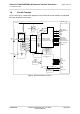
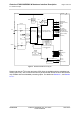
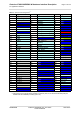
Table Of Contents
- Contents
- Tables
- Figures
- 1 Introduction
- 2 Interface Characteristics
- 2.1 Application Interface
- 2.2 RF Antenna Interface
- 2.3 GNSS Interface
- 2.4 Sample Application
- 3 Operating Characteristics
- 3.1 Operating Modes
- 3.2 Power Up/Power Down Scenarios
- 3.3 Power Saving
- 3.4 Power Supply
- 3.5 Operating Temperatures
- 3.6 Electrostatic Discharge
- 3.7 Blocking against RF on Interface Lines
- 3.8 Reliability Characteristics
- 4 Mechanical Dimensions, Mounting and Packaging
- 5 Regulatory and Type Approval Information
- 6 Document Information
- 7 Appendix

Cinterion
®
EXS62-W/EXS82-W Hardware Interface Description
2.1 Application Interface
61
t EXS62-W_EXS82-W_HID_v01.200ee 2022-09-07
Public/ Released
Page 20 of 144
2.1.2 Signal Properties
Table 2: Signal properties
Function Signal name IO Signal form and level Comment
Power
supply
BATT+
BB
I Voltage ranges:
LTE and GSM (EXS82-W only):
V
I
min = 3.3 V...V
I
max = 4.6V
LTE with GSM deactivated
V
I
min = 2.8 V...V
I
max = 4.6V
LTE with GSM deactivated; extended
voltage range:
V
I
min = 2.5 V...V
I
max = 4.8V
V
I
norm = 3.8V
I
Power Down
= 14µA
Lines of BATT+ and GND
must be connected in
parallel for supply pur-
poses because higher
peak currents may occur.
BATT+
BB
at solder pads
needs additional low ESR
47
µF capacitor (e.g, X7R
MLCC, taking DCbias
into account).
BATT+
RF
is only required
if GSM is used. In this
case BATT+
RF
at solder
pads needs additional
low ESR 150
µF capacitor
(e.g, X7R MLCC, taking
DCbias into account).
A minimum ESR value
<70mΩ is recommended.
Minimum voltage must
not fall below 3.3V
(LTE+GSM) or 2.8/2.5V
(LTE w/o GSM) including
GSM drops, ripple,
spikes. Else the module
may perform an uncon-
trolled shutdown.
If using the extended volt-
age range, i.e., down to
2.5V or up to 4.8V, the
module remains fully
functional and safe while
possibly no longer being
fully compliant with 3GPP
or other wireless stan-
dards. Please note that
the module is in this case
switched on at a voltage
of >2.65V.
Please note that if both
voltage domains and
power supply lines are
referred to - i.e., BATT+
BB
and BATT+
RF
- BATT+ is
used throughout the doc-
ument.
BATT+
RF
GSM activated
IV
I
max = 4.6V
V
I
norm = 3.8V
V
I
min = 3.3 V during Tx burst on board
Imax
= 2.16A, during Tx burst (GSM)
__|¯¯|____|¯¯|__
N Tx = n * 577µs peak current every
4.616ms
Power
supply
GND Ground Application Ground