
Specifications


Table Of Contents
- Contents
- Tables
- Figures
- 1 Introduction
- 2 Interface Characteristics
- 2.1 Application Interface
- 2.2 RF Antenna Interface
- 2.3 GNSS Antenna Interface
- 2.4 Sample Application
- 3 Operating Characteristics
- 4 Mechanical Dimensions, Mounting and Packaging
- 5 Regulatory and Type Approval Information
- 6 Document Information
- 7 Appendix
Cinterion
®
PLSx3 Hardware Interface Description
4.2 Mounting PLSx3 onto the Application Platform
99
t PLSx3_HID_v01.003 2021-03-12
Public / Released
Page 87 of 121
4.2 Mounting PLSx3 onto the Application Platform
This section describes how to mount PLSx3 onto the PCBs, including land pattern and stencil
design, board-level characterization, soldering conditions, durability and mechanical handling.
Note: To avoid short circuits between signal tracks on an external application's PCB and vari-
ous markings at the bottom side of the module, it is recommended not to route the signal tracks
on the top layer of an external PCB directly under the module, or at least to ensure that signal
track routes are sufficiently covered with solder resist.
4.2.1 SMT PCB Assembly
4.2.1.1 Land Pattern and Stencil
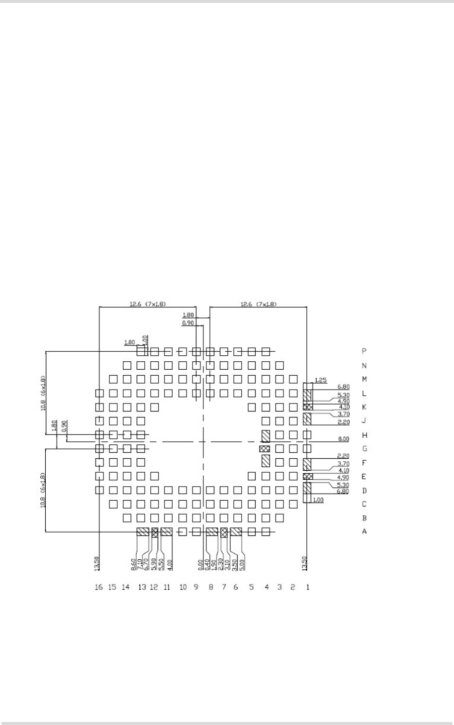
The land pattern and stencil design as shown below is based on Thales characterizations for
lead-free solder paste on a four-layer test PCB and a 110 respectively 150 micron thick stencil.
The land pattern given in Figure 33 reflects the module‘s pad layout, including signal pads and
ground pads (for pad assignment see Section 2.1.1).
Figure 33: Land pattern (top view)
The stencil designs illustrated in Figure 34 and Figure 35 are recommended by Thales as a re-
sult of extensive tests with Thales Daisy Chain modules.