
Specifications
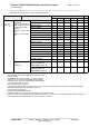
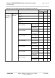
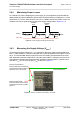
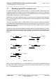
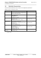
Table Of Contents
- Contents
- Tables
- Figures
- 1 Introduction
- 2 Interface Characteristics
- 2.1 Application Interface
- 2.2 RF Antenna Interface
- 2.3 GNSS Interface
- 2.4 Sample Application
- 3 Operating Characteristics
- 3.1 Operating Modes
- 3.2 Power Up/Power Down Scenarios
- 3.3 Power Saving
- 3.4 Power Supply
- 3.5 Operating Temperatures
- 3.6 Electrostatic Discharge
- 3.7 Blocking against RF on Interface Lines
- 3.8 Reliability Characteristics
- 4 Mechanical Dimensions, Mounting and Packaging
- 4.1 Mechanical Dimensions of TX62-W
- 4.2 Mechanical Dimensions of TX82-W, TX82-W-B, TX62-W-B and TX62-W-C
- 4.3 Mounting TX62/TX82 onto the Application Platform
- 4.4 Packaging
- 5 Regulatory and Type Approval Information
- 6 Document Information
- 7 Appendix

Cinterion
®
TX62-W/TX82-W Hardware Interface Description
3.4 Power Supply
120
t TX62-W_TX62-W-x_TX82-W-x_HID_v01.200d 2022-09-08
Public / Preliminary
Page 115 of 170
3.4.2 Minimizing Power Losses
For TX82-W only: When designing the power supply for your application (and with GSM en-
abled) please pay specific attention to power losses. Ensure that the input voltage V
BATT+
never
drops below 3.1V on the TX82-W board, not even in a GSM transmit burst where current con-
sumption can rise (for peak values see the power supply ratings listed in Section 3.4.1).
Figure 50: Power supply limits during transmit burst
3.4.3 Measuring the Supply Voltage (V
BATT+
)
To measure the supply voltage V
BATT+
it is possible to define two reference points GND and
BATT+. GND and BATT+ should be a test pad on the external application the module is mount-
ed on. The eternal GND reference point has to be connected to and positioned close to the
SMT application interface’s GND pad F17 and the external BATT+ reference point has to be
connected to and positioned close to the SMT application interface’s BATT+ pads G15 and
G16 (BATT+
RF
) or H15 and H16 (BATT+
BB
) as shown in Figure 51.
Figure 51: Position of reference points BATT+ and GND
Min. 3.1V
BATT+
Transmit
burst
Transmit
burst
Drop
Ripple
Reference point GND:
External test pad connected to
and positioned closely to GND
pad F17
Reference point BATT+:
External test pad connected to
and positioned closely to BATT+
pad G15, H15, H16 or G16.
External application