
User Manual

OPERATION GUIDE.
OG_CDP-02E-R-457M_v11e Circuit Design, Inc.
5
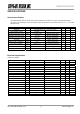
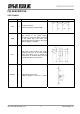
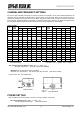
Transmitter
Item Specification Remarks MIN TYP MAX
RF output power ( 10 mW) mW 10 at 457.6 MHz 7 10 13
RF output power ( 10 mW) mW
Over all frequency range and operating temp. range
4 16
RF output power ( 1 mW) mW 0.3 1 2.6
Deviation kHz ± 2.1 PN9 2400bps / LPF=20k ± 1.6 ± 2.1 ± 2.6
DI input level for Lo V L=GND 0 0.4
DI input level for Hi V Hi=3V 3 5.5
TX carrier start up ms 50
From power on to f ± 1.5ppm
50 100
TX carrier start up at ch change
ms 35
Shift 25kHz to f ± 1.5ppm
35 85
Residual FM noise kHz 0.17
DI=L,LPF=20k
0.17 0.4
Spurious emission dBc 30 (50 ohm contact) * up to 4 th harmonics 30 40
Adjacent CH power dBc 40 PN9 2400 bps 40
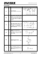
Receiver
Item Specification Remarks MIN TYP MAX
Receiver type Double superheterodyne
1st IF frequency MHz 21.7 21.7
2nd IF frequency kHz 450 450
Max. input level dBm 10 10
BER (0 error / 2556 bits)
dBm -116 PN9 2400bps -106 -116
BER (1% error) dBm -120 PN9 2400bps -120
Sensitivity 12dB / SINAD dBm -120 fm1k / dev 2.0k CCITT -120
dB 70 (1st Mix) 70
Spurious response rejections
dB 55 (2nd Mix) 55
Adjacent CH selectivity dB 60 dB (±25k) 60
Blocking dB 84 dB (+/- 1MHz) 84
Intermodulation dB
50 dB (f-200k+f-100k)
Two signal method, 1% error
50
DO output level for Hi V Hi = Vcc Z = 100 kohm or more
Vcc x0.8
Vcc
DO output level for Lo V Lo = GND Z = 100 kohm or more 0 0.7
RSSI rising time ms 30 (from PLL setup) CH shift of 25kHz 30 60
Time until valid Data-out ms 50 (from PLL setup) CH shift of 25kHz 50 100
RSSI rising time ms 50 (from PLL setup) When power ON 50 100
Time until valid Data-out ms 70 (from PLL setup) When power ON 70 140
Spurious radiation (1st Lo) dBm -57 ( 50 ohm contact) * Up to 4 th harmonics -60 -57
mV 235 (457.6 MHz) with -110 dBm 195 235 275
RSSI
mV 230 (457.6MHz) with -116 dBm 155 195 235
Notes about the specification values
BER: RF level where no error per 2556 bits is confirmed with the signal of PN9 and 2400 bps.
BER (1% error): RF level where 1% error per 2556 bits is confirmed with the signal of PN9 and 2400 bps.
Spurious response, CH selectivity: Jamming signal used in the measurement is unmodulated.
Intermodulation: Ratio between the receiver input level with BER 1% and the signal level (PN9 2400 bps) added at the
points of "Receiving frequency -200 kHz" + "Receiving frequency -100 kHz" with which BER 1% is
achieved.
Time until valid Data-out: Valid DO is determined at the point where Bit Error Rate meter starts detecting the signal of
2400 bps, 1010 repeated signal.
Conditions:
All specifications are specified based on the data measured in a shield room using the PLL setting controller
board prepared by Circuit Design.
Measurement equipment SG = ANRITSU communication analyzer MT2605
Spectrum analyzer = ANRITSU MS2663G / BER measure = ANRITSU MP1201G