OPERATION GUIDE UHF Narrow band multi channel transceiver LMD-400-R 438-442/458-462 MHz Operation Guide Version 1.0 (May.2010) CIRCUIT DESIGN, INC., 7557-1 Hotaka, Azumino Nagano 399-8303 JAPAN Tel: + +81-(0)263-82-1024 Fax: + +81-(0)263-82-1016 e-mail: info@circuitdesign.jp http://www.circuitdesign.
OPERATION GUIDE CONTENTS GENERAL DESCRIPTION & FEATURES ...........................3 SPECIFICATIONS ...............................................................4 PIN DESCRIPTION .............................................................6 BLOCK DIAGRAM...............................................................8 DIMENSIONS......................................................................9 PLL IC CONTROL .............................................................10 PLL IC control .............
OPERATION GUIDE GENERAL DESCRIPTION & FEATURES General Description The LMD-400-R (438-442 MHz & 458-462 MHz) is a synthesized multi channel transceiver module for use under the EN 300 113 Land mobile services. This simple, compact and low power transceiver is designed for embedding in user equipment and suitable for various low power industrial telecontrol and telemetry applications requiring high performance and reliability.
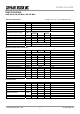
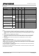
OPERATION GUIDE SPECIFICATIONS LMD-400-R 438-442 MHz / 458-462 MHz General characteristics All ratings at 25 +/-10 °C unless otherwise noted Item Applicable standard Communication method Emission class Modulation type Units Operating frequency range MHz Operation temperature range Storage temperature range Aging rate Initial frequency tolerance Dimensions Weight °C °C ppm ppm mm g MIN TYP MAX EN 300 113 Simplex, Half-duplex F1D GFSK 438.000 442.000 458.000 462.000 -20 60 -30 75 -1 1 -1.5 1.
OPERATION GUIDE Receiver part Item Receiver type 1st IF frequency 2nd IF frequency Maximum input level BER (0 error/2556 bits) *1 BER (1 % error) *2 Sensitivity 12dB/ SINAD Co-channel rejection Spurious response rejection *3 dB Adjacent CH selectivity *3 dB MIN TYP MAX Double superheterodyne 21.
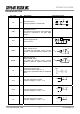
OPERATION GUIDE PIN DESCRIPTION Pin name I/O Description Equivalent circuit 47P SAW FILTER RF I/O RF RF input terminal Antenna impedance nominal 50 Ω 100nH GND GND I GROUND terminal The GND pins and the feet of the shield case shoud be connected to the wide GND pattern. VCC 2.8V VCC TXSEL I Power supply terminal DC 3.0 to 5.5 V I TX select terminal GND = TXSEL active To enable the transmitter circuits, connect TXSEL to GND and RXSEL to OPEN or 2.8 V.
OPERATION GUIDE 2.8V LD O PLL lock/unlock monitor terminal Lock = H (2.8 V), Unlock = L (0 V) 2K LD MB15E03 102 RSSI O Received Signal Strength Indicator terminal 2.8V DO DI O I OG_LMD-400-R-AB_v10e Data output terminal Interface voltage: H=2.8V, L=0V 10K 2K DO 102 Data input terminal Interface voltage: H=2.8V to Vcc, L=0V Input data pulse width Min.100 µs Max. 15 ms 7 Circuit Design, Inc.
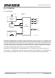
OPERATION GUIDE. BLOCK DIAGRAM OG_LMD-400-R-AB_v10e 8 Circuit Design, Inc.
OPERATION GUIDE. DIMENSIONS OG_LMD-400-R-AB_v10e 9 Circuit Design, Inc.
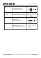
OPERATION GUIDE . PLL IC CONTROL z PLL IC control Figure 1 up to 1200MHz VCO 2kohm Voltage Controled Oscillator Fin CLK 2kohm Data Xf in 2kohm LE GND LPF PLL Do +2.8v LE PS ZC VCC 2kohm 21.25MHz DATA MB15E03SL Vp TCXO Reference Oscillator CLK LD/f out OSCout P OSCin R LD STD-302 Control pin name #:Control v oltage = +2.8v LMD-400-R is equipped with an internal PLL frequency synthesizer as shown in Figure 1.
OPERATION GUIDE z . How to calculate the setting values for the PLL register The PLL IC manual shows that the PLL frequency setting value is obtained with the following equation.
OPERATION GUIDE z . Method of serial data input to the PLL After the RF channel table plan is decided, the data needs to be allocated to the ROM table and read from there or calculated with the software. Together with this setting data, operation bits that decide operation of the PLL must be sent to the PLL. The operation bits for setting the PLL are as follows. These values are placed at the head of the reference counter value and are sent to the PLL. 1. CS: Charge pump current select bit CS = 0 +/-1.
OPERATION GUIDE . TIMING CHART Control timing in a typical application is shown in Figure 3. Initial setting of the port connected to the radio module is performed when power is supplied by the CPU and reset is completed. MOS-FET for supply voltage control of the radio module, RXSEL and TXSEL are set to inactive to avoid unwanted emissions. The power supply of the radio module is then turned on.
OPERATION GUIDE . LMD-400 Figure 3: Timing diagram for STD-302 Status immediately after pow er comes on. Normal status Channel change No channel change CPU Pow er on LMD-400 STD-302 Power on #:3 Pow er on Receiv e mode Receiv e mode Receiv e mode activ e period activ e period activ e period Activ e period RXSEL CPU control, CH change & Data rec.
OPERATION GUIDE PLL FREQUENCY SETTING DATA REFERENCE Example : Setting from 458.000 MHz to 458.6125 MHz Parameter name Value Phase Comparing Frequency Fcomp [kHz] Start Channel Frequency Fch [MHz] Channel Step Frequency [kHz] Number of Channel Prescaler M 12.5 458.000 12.5 50 64 Parameter name Reference Frequency Fosc [MHz] Offset Frequency Foffset [MHz] Value 21.25 21.
OPERATION GUIDE 458.3875 436.6875 436.6875 34935 545 55 458.4000 436.7000 436.7000 34936 545 56 57 458.4125 436.7125 436.7125 34937 545 458.4250 436.7250 436.7250 34938 545 58 458.4375 436.7375 436.7375 34939 545 59 60 458.4500 436.7500 436.7500 34940 545 458.4625 436.7625 436.7625 34941 545 61 458.4750 436.7750 436.7750 34942 545 62 63 458.4875 436.7875 436.7875 34943 545 458.5000 436.8000 436.8000 34944 436.8125 436.8125 34945 546 546 0 458.
OPERATION GUIDE Regulatory compliance information Regulatory compliance of the LMD-400-R The LMD-400-R is designed for embedding in other equipment (Products incorporating the LMD-400-R are henceforward referred to as final products). The European regulation applicable to the LMD-400-R is the R&TTE Directive 1999/5/EC. The conformity assessment for the LMD-400-R was completed in accordance with the R&TTE Directive Annex III procedures, and the Declaration of Conformity is attached to this manual.
OPERATION GUIDE Regulatory compliance information OG_LMD-400-R-AB_v10e 18 Circuit Design, Inc.
OPERATION GUIDE Important notice • Customers are advised to consult with Circuit Design sales representatives before ordering. Circuit Design believes the provided information is accurate and reliable. However, Circuit Design reserves the right to make changes to this product without notice. • Circuit Design products are neither designed nor intended for use in life support applications where malfunction can reasonably be expected to result in significant personal injury to the user.
OPERATION GUIDE REVISION HISTORY Version 0.9 1.0 Date Jan. 2010 May. 2010 OG_LMD-400-R-AB_v10e Description Preliminary DOC added、specification reviewed 20 Remark Circuit Design, Inc.