OPERATION GUIDE UHF Narrow band multi channel transceiver LMD-401 Operation Guide Version 1.0 (May. 2020) CIRCUIT DESIGN, INC., 7557-1 Hotaka, Azumino Nagano 399-8303 JAPAN Tel: + +81-(0)263-82-1024 Fax: + +81-(0)263-82-1016 e-mail: info@circuitdesign.jp http://www.circuitdesign.
OPERATION GUIDE CONTENTS GENERAL DESCRIPTION & FEATURES ........................... 3 SPECIFICATIONS ............................................................... 4 PIN DESCRIPTION ............................................................. 6 BLOCK DIAGRAM............................................................... 8 DIMENSIONS ...................................................................... 9 PLL IC CONTROL ............................................................. 10 PLL IC control ......
OPERATION GUIDE GENERAL DESCRIPTION & FEATURES General Description The LMD-401 is a synthesized multi-channel transceiver module for use under the Land Mobile Radio services (FCC Part 90, ISED RSS-119). This simple, compact and low power transceiver is designed for embedding in user's portable or fixed equipment and suitable for various low power industrial telecontrol and telemetry applications requiring high performance and reliability.
OPERATION GUIDE SPECIFICATIONS LMD-401 All ratings at 25 +/-10 °C unless otherwise noted General characteristics Item Applicable standard Communication method Emission class Modulation type Operating frequency range Operation temperature range Storage temperature range Aging rate Initial frequency tolerance Dimensions Weight Units MHz °C °C ppm ppm mm g MIN TYP MAX FCC Part 90.217, ISED RSS-119 Simplex, Half-duplex F1D GFSK 458.000 462.
OPERATION GUIDE Receiver part Item Receiver type 1st IF frequency 2nd IF frequency Maximum input level BER (0 error/2556 bits) *1 BER (1 % error) *2 Sensitivity 12dB/ SINAD Co-channel rejection MHz kHz dBm dBm dBm dBm dB MIN TYP MAX Double superheterodyne 21.7 450 10 -113 -116 -116 -7 PN 9 4800bps PN 9 4800bps fm1 k/ dev 2.
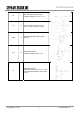
OPERATION GUIDE PIN DESCRIPTION Pin name I/O Description Equivalent circuit RF I/O RF input terminal Antenna impedance nominal 50 Ω GND I GROUND terminal The GND pins and the feet of the shield case shoud be connected to the wide GND pattern. VCC I Power supply terminal DC 3.0 to 5.5 V I TX select terminal GND = TXSEL active To enable the transmitter circuits, connect TXSEL to GND and RXSEL to OPEN or 2.8 V.
OPERATION GUIDE LE I PLL data setting input terminal Interface voltage H = 2.8 V, L = 0 V LD O PLL lock/unlock monitor terminal Lock = H (2.8 V), Unlock = L (0 V) RSSI O DO O Data output terminal Interface voltage: H=2.8V, L=0V I Data input terminal Interface voltage: H=2.8V to Vcc, L=0V Input data pulse width Min.100 μs Max. 15 ms DI OG_LMD-401_v10e Received Signal Strength Indicator terminal 7 Circuit Design, Inc.
OPERATION GUIDE. BLOCK DIAGRAM RSSI Butterworth character Active Filter RX2.8V RX2.8V RX2.8V SAW-FILTER SAW-FILTER DATA SLICER/AMP RX2.8V RX2.8V MCF 21.7MHz± 7.5kHz DO IF-IC LNA AFOUT Down Converter IF FILTER 450kHz ± 4.5kHz DISC 450kHz VCO2.8V DATA CLK LE LD VCO2.8V HPF(L・ C) RF DIS(L・ C・ R) ATT(R) RF SW BUFF PLL VCO2.8V VCO Electrostatic protection GND TX2.8V 21.25MHz Local adj. TX2.8V VCO2.8V Power adj. TC-XO (with VC) SAW-FILTER VCO2.8V VCO2.8V VCO2.
OPERATION GUIDE. DIMENSIONS Reference hole position for PCB mounting (Top view) OG_LMD-401_v10e 9 Circuit Design, Inc.
OPERATION GUIDE . PLL IC CONTROL PLL IC control Figure 1 up to 1200MHz VCO 2kohm Voltage Controled Oscillator Fin CLK Xf in Data 2kohm 2kohm GND LPF LE PLL Do +2.8v LE PS VCC ZC 2kohm 21.25MHz DATA MB15E03SL DHL612 Vp Reference Oscillator CLK LD/f out OSCout P OSCin R LD STD-302 LMD-401 Control pin name connector pin name #:Control v oltage = +2.8v LMD-401 is equipped with an internal PLL frequency synthesizer as shown in Figure 1.
OPERATION GUIDE . How to calculate the setting values for the PLL register The PLL IC manual shows that the PLL frequency setting value is obtained with the following equation.
OPERATION GUIDE . Method of serial data input to the PLL After the RF channel table plan is decided, the data needs to be allocated to the ROM table and read from there or calculated with the software. Together with this setting data, operation bits that decide operation of the PLL must be sent to the PLL. The operation bits for setting the PLL are as follows. These values are placed at the head of the reference counter value and are sent to the PLL. 1. CS: Charge pump current select bit CS = 0 +/-1.
OPERATION GUIDE . TIMING CHART Control timing in a typical application is shown in Figure 3. Initial setting of the port connected to the radio module is performed when power is supplied by the CPU and reset is completed. MOS-FET for supply voltage control of the radio module, RXSEL and TXSEL are set to inactive to avoid unwanted emissions. The power supply of the radio module is then turned on.
OPERATION GUIDE . LMD-401 Figure 3: Timing diagram for STD-302 Status immediately after pow er comes on. Normal status Channel change No channel change CPU Pow er on LMD-401 STD-302 Power on #:3 Pow er on Receiv e mode Receiv e mode Receiv e mode activ e period activ e period activ e period Activ e period RXSEL CPU control, CH change & Data rec.
OPERATION GUIDE PLL FREQUENCY SETTING DATA REFERENCE Example : Setting from 458.000 MHz to 458.6125 MHz Parameter name Value Phase Comparing Frequency FCOMP [kHz] Start Channel Frequency FCH [MHz] Channel Step Frequency [kHz] Number of Channel Prescaler M 12.5 458.000 12.5 50 64 Parameter name Reference Frequency FREF [MHz] Offset Frequency FOFFSET [MHz] Value 21.25 21.
OPERATION GUIDE 458.3625 458.3750 436.6625 436.6750 436.6625 436.6750 34933 545 53 34934 545 54 55 458.3875 436.6875 436.6875 34935 545 458.4000 436.7000 436.7000 34936 545 56 458.4125 436.7125 436.7125 34937 545 57 58 458.4250 436.7250 436.7250 34938 545 458.4375 436.7375 436.7375 34939 545 59 458.4500 436.7500 436.7500 34940 545 60 61 458.4625 436.7625 436.7625 34941 545 458.4750 436.7750 436.7750 34942 545 62 458.4875 436.7875 436.
OPERATION GUIDE Regulatory compliance information Regulatory Statement for FCC The LMD-401 complies with the FCC Part 90. Labelling: The LMD-401 is labeled as below. FCC ID: V9X-LMD401 The proposed FCC ID label format is to be placed on the module. If FCC ID is not visible when the module is installed into the system, "Contains FCC ID: V9X-LMD401” shall be placed on the outside of final host system.
OPERATION GUIDE Licensing of end-use products LMD-401 holds equipment authorization for transmitting equipment under Title 47 of the Code of Federal Regulations Part 90. (FCC Identifier: V9X-LMD401) This shall be the only guarantee of Circuit Design Inc for compliance with FCC regulations. Those who integrate LMD-401 in a system and operate the radio system in the United States are required to apply for a user station license before the equipment can be operated.
OPERATION GUIDE Regulatory Statement for Industry Canada The LMD-401 complies with the RSS-119. Caution: Any changes or modifications not expressly approved by the party responsible for product compliance could void the user’s authority to operate the equipment. Labelling: The LMD-401 is labeled as below. IC Number: 6079A-LMD401 The proposed IC Number label format is to be placed on the module.
OPERATION GUIDE users/stations. As local frequency management issues are involved in licensing, Circuit Design Inc shall not be held liable for failure in obtaining the station license. Circuit Design Inc recommends users to contact a certified frequency coordinator in the region in advance to confirm whether or not a license can be granted. OG_LMD-401_v10e 20 Circuit Design, Inc.
OPERATION GUIDE Important notice Customers are advised to consult with Circuit Design sales representatives before ordering. Circuit Design believes the provided information is accurate and reliable. However, Circuit Design reserves the right to make changes to this product without notice. Circuit Design products are neither designed nor intended for use in life support applications where malfunction can reasonably be expected to result in significant personal injury to the user.
OPERATION GUIDE REVISION HISTORY Version 1.0 Date May. 2020 OG_LMD-401_v10e Description 22 Remark Circuit Design, Inc.