
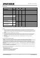
Specifications

OG_STD-302N-R_v15e Circuit Design, Inc.
6
OPERATION GUIDE
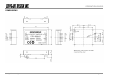
PIN DESCRIPTION
Pin name I/O Description Equivalent circuit
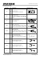
RF I/O
RF input terminal
Antenna impedance nominal 50 Ω
GND I
GROUND terminal
The GND pins and the feet of the shield case
shoud be connected to the wide GND
pattern.
VCC I
Power supply terminal
DC 3.0 to 5.5 V
TXSEL I
TX select terminal
GND = TXSEL active
To enable the transmitter circuits, connect
TXSEL to GND and RXSEL to OPEN or 2.8
V.
RXSEL I
RX select terminal
GND= RXSEL active
To enable the receiver circuits, connect
RXSEL to GND and TXSEL to OPEN or 2.8
V.
AF O
Analogue output terminal
There is DC offset of approx. 1 V.
Refer to the specification table for amplitude
level.
CLK I
PLL data setting input terminal
Interface voltage H = 2.8 V, L = 0 V
DATA I
PLL data setting input terminal
Interface voltage H = 2.8 V, L = 0 V
LE I
PLL data setting input terminal
Interface voltage H = 2.8 V, L = 0 V
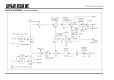
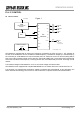
100nH
47P
RF
GND
SAW FILTER
REG
VCC
47P
10µ
22µ
47P
2.8V
2.8V
10
TXSEL
2.8V
20K
2.8V
10
RXSEL
2.8V
20K
MB15E03
CLK
2K
MB15E03
DATA
2K
MB15E03
LE
2K