AN186 Application Note BRINGING UP THE EP72/73XX DEVICE Note: Cirrus Logic assumes no responsibility for the attached information which is provided “AS IS” without warranty of any kind (expressed or implied). P.O. Box 17847, Austin, Texas 78760 (512) 445 7222 FAX: (512) 445 7581 http://www.cirrus.com Copyright Cirrus Logic, Inc.
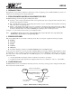
AN186 TABLE OF CONTENTS 1. 2. 3. 4. 5. 6. 7. 8. 9. INTRODUCTION ....................................................................................................................... 3 THE SUPPORTED POWER MANAGEMENT STATES ........................................................... 3 THE DEGLITCHER ................................................................................................................... 3 WAKEUP DELAYS ............................................................................
AN186 1. INTRODUCTION This application note describes in detail the recommended procedure for applying power to the EP72/73XX device, and how to transition from the Standby State into the Operating State. 2. THE SUPPORTED POWER MANAGEMENT STATES The EP72/73XX supports the following Power Management States: l Operating — The normal program Execution State is the Operating State; this is a full performance State where all of the clocks and peripherals are enabled.
AN186 4.1 Power-up Delay - 100us Upon power-up, the EP72/73XX is in an unknown state. It must first be reset by the power-on reset signal (nPOR). nPOR (active low) should be held low until the power supply reaches its operational voltage to initialize the EP72/73XX properly, and to allow the RTC to stabilize. Since the power-on reset operates asynchronously to the system clock, it is not required to wait until the system clock is stabilized.
AN186 Notes: 1. The use of the keypress interrupt is disabled after any of the three available resets become active (i.e. nPOR, nURESET, or nPWRFL) due to the fact that the KBWEN bit is cleared by default. Therefore, a keypress cannot wake-up the device after a cold boot or power fail. 2. When the EP72/73XX is in the Standby State, the nPWRFL signal is disabled. It cannot be used to reset the device.
AN186 5. LOCK-OUT PERIOD DELAYS These delays can be described as the amount of delay from when the WAKEUP signal first rises, until the CPU starts fetching instructions. There are two cases of these wakeup delays in the EP72/73XX. One case is the cold boot that can happen after power-up, in changing a battery, or a power failure. The second instance occurs after software has forced the device into the Standby State. In both cases, the internal system clock is turned off to save power consumption.
AN186 7. WAKEUP AND nURESET CAVEAT When the WAKEUP signal is used to exit the Standby State, nURESET must be held in its inactive state. During the period of time between when the WAKEUP signal becomes active and the EP72/73XX device completely enters the Operating State, nURESET must remain inactive. If nURESET becomes active during this period of time, the device may lock up, and the only recovering mechanism is to perform a complete reset. This will have to be accomplished by using the nPOR signal.
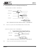
AN186 8. TIMING DIAGRAMS 8.1 Timing Diagram in the case of a Cold Boot Power Supply 100us min. width nPOR (input) See note 1. WAKEUP See note 3 22sec sec max. min See note 3 125us min. width (62-125us) CLKEN (output) See note 4. Stable clock OSC/PLL Internal RUN (125-250ms) Wakeup delay delay Instruction fetches Figure 3. Timing Diagram for the Case of a Cold Boot Notes: 1.
AN186 8.2 Timing Diagrams for the Case of Wakeup from Standby State A. External OSC(13Mhz) with “CLKEN” on “RUN/CLKEN” pin WAKEUP (input) (62-125us) CLKEN (output) Stable clock OSC (125-250ms) Internal RUN Instruction fetches Figure 4. Timing Diagram, External OSC(13 MHz) with “CLKEN” on ‘”RUN/CLKEN” Pin Note: In Figure 4, the system assumes that the CLKEN pin enables the external oscillator. B.
AN186 C. PLL Clock with “CLKEN” on “RUN/CLKEN” pin WAKEUP (input) (62-125us) CLKEN (output), Stable clock PLL (125-250ms) Internal RUN Instruction fetches Figure 6. Timing Diagram, PLL Clock with “CLKEN” on “RUN/CLKEN” Pin D. PLL Clock with “RUN” on “RUN/CLKEN” Pin WAKEUP (input) Stable clock PLL RUN (125-250ms) Instruction fetches Figure 7.
AN186 9. AUTOMATIC WAKEUP CIRCUIT 47k R1 Vdd 14 1 U1A 2 2 U2 1 3 7 WAKEUP 74LCX14 74LCX02 C1 0.1uF WAKEUP_DIS Unused GPIO pin R2 47k Figure 8.