AN187 Application Note USING THE EP72/7312 TO IMPLEMENT A SOFT MODEM P.O. Box 17847, Austin, Texas 78760 (512) 445 7222 FAX: (512) 445 7581 http://www.cirrus.com Copyright Cirrus Logic, Inc.
AN187 TABLE OF CONTENTS 1. 2. 3. 4. 5. INTRODUCTION ....................................................................................................... 3 EP72/7312 DIGITAL AUDIO INTERFACE (DAI) ................................................ 3 SI3034 DAA CHIP SET .............................................................................................. 4 INTERFACING THE EP72/7312 TO THE SI3034 .................................................
AN187 1. INTRODUCTION As the world of PDAs and other hand-held devices evolves, more and more of these products desire the support of an analog modem to communicate with the Internet. Today, the use of modems constitutes only a small market share. However, the desire for modem support is growing dramatically. Due to this fact, this application note has been created.
AN187 SCLK is derived from MCLK. It is ½ MCLK. In the default mode, the DAI is in the Master mode. In this mode it generates its own MCLK clock. It is 9.216 MHz. Thus SCLK becomes 4.608 MHz. For applications that need SCLK to be different speed, the DAI can be configured to be in the Slave mode. In this mode, MCLK is provided from an external source via the MCLK pin. When in the Slave mode, the DAI will receive its master clock from the MCLK pin, and then divide it in half to create SCLK.
AN187 4. INTERFACING THE EP72/7312 TO THE SI3034 The EP7312 can generate a 4.096 MHz internal clock. But, in the EP7212, the DAI interface can only provide a fixed internal clock source of 9.216 MHz when in Master mode. Because this is incompatible with the clock rate needed by the DAA, the DAI has to be configured for Slave mode. An external clock source of 4.096 MHz is thus connected to the DAI MCLK pin, which internally will be halved to create its SCLK.
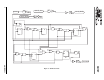
Figure 1.
nSCLK_also 11 nSCLK 18 I22 27 LRCK_DLYD I24 6 SCLK_DLYD I23 I21 I4 I3 D Q I6 I11 I17 D Q I12 I13 I18 I10 D D Q I19 I8 I5 I7 I9 I14 D Q I15 Q I2 I16 3 nFSYNC AN187 AN187REV1 Figure 2.
AN187 5.
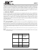
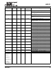
AN187 P-Terms Fan-in Fan-out Type Name (attributes) 2/2 2 1 node N_9 N_9 = (N_11 & !N_12 # !N_11 & N_12) N_10 Reverse Polarity — !N_9 = (!N_11 & !N_12 # N_11 & N_12) N_10 = (N_19 & N_9) 1/2 2 1 node Equations Reverse Polarity — !N_10 = (!N_19 # !N_9) 1/3 3 1 node N_11 1/1 1 1 node N_12.D 1/1 1 1 node N_12.C N_11 = (N_16 & N_15 & N_13) Reverse Polarity — !N_11 = (!N_15 # !N_16 # !N_13) N_12.D = (N_10) Reverse Polarity — !N_12.D = (!N_10) N_12.
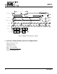
AN187 16 cycles nFSYNC 64 cycles 64 cycles LRCK LRCK_DLYD SCLK nSCLK SDOUT SDIN D15 D14 D1 D15 D14 D1 D0 Figure 3. EP72/7312 to Si3035 Interface Signals 6. SILICON LABORATORIES CONTACT INFORMATION Silicon Laboratories, Inc. 4635 Boston Lane Austin, Texas 78735 Phone: 1-877-444-3032 Email: SiDAAinfo@silabs.com Web site: www.silabs.
• Notes •