
Manual


AN187
AN187REV1 3
1. INTRODUCTION
As the world of PDAs and other hand-held devices evolves, more and more of these products desire the support of an analog
modem to communicate with the Internet. Today, the use of modems constitutes only a small market share. However, the desire
for modem support is growing dramatically. Due to this fact, this application note has been created.
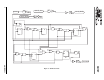
This application note describes how the ARM720T™ processor, DRAM controller, and the Digital Audio Interface (DAI)
integrated into the Cirrus Logic EP72/7312 embedded processor can be used to implement a V.90 softmodem solution.
Used in conjunction with the EP72/7312 are the following components:
n V.90 softmodem and driver code
n Silicon Laboratories™ Si3034 DAA chip set
n A simple PLD, used to implement the interface logic between the DAI and the Si3035 chip set.
Schematics and a timing diagram are provided to explain the characteristics of this interface.
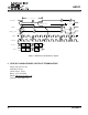
2. EP72/7312 DIGITAL AUDIO INTERFACE (DAI)
Within the EP212 is an integrated Digital Audio Interface (DAI). This interface was implemented to support high quality stereo
audio transmission and reception. However, it can be used to support other functions, like a softmodem. The interface consists
of five signals:
n LRCK Left/right frame sync; output only
n SCLK Bit clock; equals ½ MCLK; there are 128 bits-per-frame; output only
n MCLK 2x oversampled clock; input when in Slave mode
n SDOUT Digital audio data out; output
n SDIN Digital audio data in; input
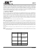
An example of the timing interface generated by the DAI for a typical audio application is shown in Figure 1.
The data uses the MSB/Left Justified format. This means that the data is clocked in/out immediately after the frame sync
(LRCK) changes levels. The data is left justified, with the MSB first. This is slightly different than the I2S format, where the
data is delayed by one clock after the frame sync changes levels. Each frame is 128 bits long. Thus each channel (i.e., left and
right) is 64 bits wide. The frame size and duty cycle of the signal LRCK cannot be configured in the EP72/7312. 'The frame
size in the EP7312 can be configured for either 128 or 64 bits per frame, but this is not relevent for this application.
Figure 1. Example Timing Interface Generated by the DAI
Figure 1 Parameters: MSB/Left Justified format
Mclock = 256
fs
, bit rate = 128
fs
LRCK
SCLK
Left Channel
Right Channel
SDATA +3 +2 +1 LSB+5 +4
MSB-1-2-3-4-5
+3 +2 +1 LSB+5 +4
MSB-1 -2 -3 -4
SDATA +3 +2 +1 LSB+5 +4
MSB-1-2-3-4-5
+3 +2 +1 LSB+5 +4
MSB-1 -2 -3 -4
SDATAI +3 +2 +1 LSB+5 +4MSB-1-2-3-4-5 +3 +2 +1 LSB+5 +4MSB-1 -2 -3 -4
O
128 clocks