
Manual


AN187
4 AN187REV1
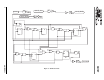
SCLK is derived from MCLK. It is ½ MCLK. In the default mode, the DAI is in the Master mode. In this mode it generates its
own MCLK clock. It is 9.216 MHz. Thus SCLK becomes 4.608 MHz. For applications that need SCLK to be different speed,
the DAI can be configured to be in the Slave mode. In this mode, MCLK is provided from an external source via the MCLK
pin. When in the Slave mode, the DAI will receive its master clock from the MCLK pin, and then divide it in half to create
SCLK. In this application of the softmodem, we will need to use this Slave mode, and provide a 4.096 MHz clock source into
the MCLK pin. SCLK and LRCK are always configured as outputs regardless of the DAI mode setting. The data is latched in
on the positive going edge of the SCLK, and is clocked out on the negative going edge.
3. SI3034 DAA CHIP SET
The Silicon Laboratories Si3034 is an integrated Direct Access Arrangement (DAA) that provides a programmable line
interface to meet global telephone line interface requirements. Programmable features include AC and DC terminations, ringer
impedance and ringer threshold. Also supported is billing tone detection, polarity reversal, pulse dialing, and on-hook line
monitoring. Available in two 16-pin small outline packages, it eliminates the need for an analog front-end (AFE), an isolation
transformer, relays, opto-isolators, and a 2- to 4-wire hybrid circuit. This Si3034 chip set runs at either 3.3v or 5V, and
dramatically reduces the number of discrete external components required to achieve compliance with global regulatory
requir.ements. If only compliance to North American and Japanese standards are required, the Si3035 DAA may be used instead
of the Si3034 global DAA
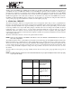
The DAA communication interface consists of the signals described in Table 1.
NOTE: There are other signals on the DAA as well. Please refer to the
Si3034
or
Si3035 Data Sheet
for their oper-
ation and configuration.
The Si3034/35 transfers data in a 16-bit halfword format. Data is transferred using the same MSB/Left Justified format as the
EP72/7312's DAI. It uses a 256-bit frame size. In this 256-bit frame are two 128-bit-long time slots: primary and secondary.
The two time slots are delineated by the rising edge of nFSYNC. Thus nFSYNC toggles twice per frame. The primary time slot
is used to transfer telephony data. The secondary time slot is used as a control channel between the Host and the DAA. It can
be used to change the default configuration settings of the chip set. Refer to the Si3034 or the Si3035 Data Sheet for more
information.
The data is latched on the negative going edge of SCLK, and is clocked out on the positive going edge. This is the opposite of
the DAI.
NOTE: Carefully follow the instructions in the
Si3034/35 Data Sheet
to program and implement the device properly
in your system design.
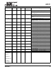
Signal Name Purpose Activity
nFSYNC Frame Sync Output in Master
mode, input in
Slave mode
SCLK Bit Clock Output when in
Master mode, no
connect in Slave
mode
MCLK Master
clock
1x SCLK, used as
input to create bit
clock
SD0 Data out
SDI Data in
Table 1. DAA Interface Signals