
Manual


AN187
AN187REV1 5
4. INTERFACING THE EP72/7312 TO THE SI3034
The EP7312 can generate a 4.096 MHz internal clock. But, in the EP7212, the DAI interface can only provide a fixed internal
clock source of 9.216 MHz when in Master mode. Because this is incompatible with the clock rate needed by the DAA, the DAI
has to be configured for Slave mode. An external clock source of 4.096 MHz is thus connected to the DAI MCLK pin, which
internally will be halved to create its SCLK. Since the DAI and DAA logic need to be synchronized, SCLK outputting from the
DAI can be used (after inverted) as the MCLK input into the DAA.
For the modem to support the V.90 protocol it needs to transfer each sample of data at a rate of 8 kHz. This means that each
frame must be transferred at this rate. Since the frame size of the DAA is 256 bits-per-frame, this equates to a bit rate of 2.048
MHz. Therefore, a clock source of 2.048 MHz should be connected to the MCLK pin of the DAA. In order to achieve the correct
frame rate from a 2.048 MHz MCLK input, the DAA also needs to be configured in Slave mode.
With the DAA running in Slave mode, MCLK and nFSYNC have to be supplied to the DAA. It has already been stated above
how MCLK gets created, however now the creation of nFSYNC needs to be discussed. The nFSYNC signal requires nFSYNC
to be low during the 16 bit data transfer, and high all other times. This does not comply with the I2S like interface. So a circuit
has been created to shape the frame sync signal generated by the DAI (i.e. LRCK), to meet the timing requirements of the frame
sync signal input required by the DAA (i.e. nFSYNC). This circuit counts 16 bit cycles after LRCK goes high, and forces the
created nFSYNC signal high after these 16 cycles. It keeps nFSYNC high, until LRCK goes high again. This circuit has been
implemented using a low cost small CPLD. The Lattice ispMACH 4A CPLD (exact part number: M4A3-32/32-10VC) device
is used. To meet the setup time spec of the internal D-FFs, LRCK must be delayed. This is accomplished by using two spare
74LVX14 inverters in series with LRCK prior to it entering the CPLD.
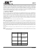
In high volume (500k), the device is between 50 cents and $1.00.
To allow for the lowest speed ispMACH device (i.e., 10ns), SCLK created for the DAA is delayed through the CPLD. This
allows the critical spec for the DAA (i.e., Td1 and Td2; Delay Time, SCLK high to nFSYNC high, and SCLK high to nFSYNC
low, respectively) to be met easily. The resulting signal is called SCLK_DLYD. It should be connected to the DAA’s MCLK pin.
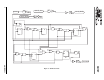
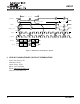
A schematic breakdown of the entire circuit is provided in Figure 1, “Circuit Schematic,” on page 6. The schematics for the
CPLD only is shown in Figure 2, “CPLD Schematic,” on page 7.
NOTE: It is required to connect nSCLK to two separate input pins on the CPLD: 1). The input clock, and 2). A gen-
eral purpose input. This was necessary to be able to route nSCLK in and out of the device to create the
signal SCLK_DLYD.
The CPLD equations compiled from the schematics are provided in , and the timing diagram is provided in Figure 3,
“EP72/7312 to Si3035 Interface Signals,” on page 10. The user should read carefully through the ispMACH Data Sheet to
program and implement the device properly in the system design.