
User guide


Table Of Contents
AN375
18 AN375REV4
4 Design Example
The Cirrus Logic CRD1615-8W reference design is used for the design example. The required operating parameters
for the analytical process are outlined in the table below.
Notes: 1. It is desirable to use a power FET that does not exceed 600V breakdown.
2. Experience shows that a minimum hold current of 60mA is required for wide dimmer compatibility.
3. Preliminary efficiency estimate is 82%
4. Rectifying diode voltage V
F
is equal to 0.9V
5. To assure that the switching frequency second harmonic does not contribute against the 150kHz EMI limit, set the
maximum switching frequency to 66kHz counting on some attenuation due to the EMI receiver selectivity.
Step 1) Determine I
IN(CC)
Use Equation 3 on page 8 to calculate dimmer current I
fb
at maximum output power and minimum input
voltage. See Equation 26:
Since current I
fb
is equal to 107mA and is greater than current I
hold
, which is equal to 60mA, use Equation 4
on page 9 to set current I
IN(CC)
equal to 107mA. See Equation 27:
Step 2) Select an Appropriate FET
For a zener diode snubber circuit, calculate the maximum peak line voltage V
INPK(max)
using Equation 28:
Using a 250V zener as a clamp device sets the maximum zener clamp voltage V
Zener(max)
to 275V (+10%
tolerance), leaving 138V of margin voltage V
Margin
to a 600V FET. Using an analytical approach to partition
zener voltage V
Zener
into reflected voltage V
Reflected
and overshoot voltage (V
Zener
- V
Reflected
) requires
assumptions on the switching details. It is recommended to choose reflected voltage V
Reflected
to equal
approximately 70% of zener voltage V
Zener
. Reflected voltage V
Reflected
is set to 165.6V, which allows for a
practical transformer turns ratio and leaves approximately 110V of overshoot to dissipate the leakage
inductance energy. The actual overshoot range is from 82V to 137V, depending on the zener clamp tolerance.
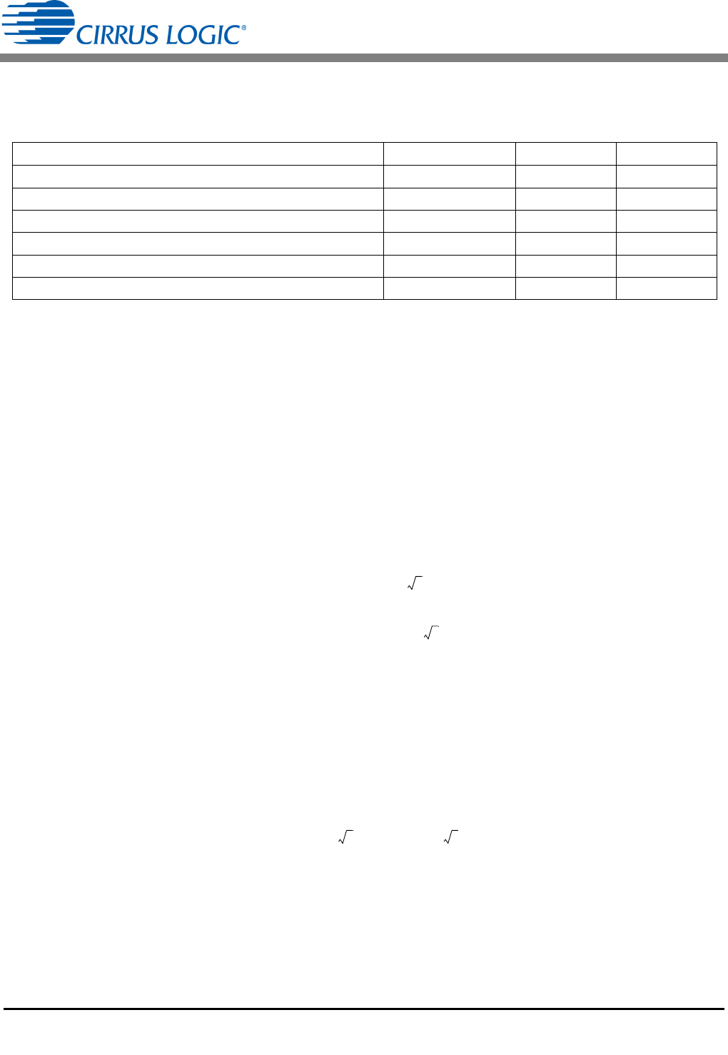
Parameters Symbol Value Tolerance
Output Power
P
OUT
7.0W
AC Line Input Voltage
V
IN
120V ±10%
Output Voltage
V
OUT
27.9V ±0%
Load Current
I
OUT
250mA
AC Line Frequency
f
IN
60Hz
Maximum Switching Frequency*
F
SWFREQ(90°)
66kHz
* Increasing switching frequency F
sw
may reduce the size of the magnetics but increase switching losses in the FET and
transformer.
I
fb
P
OUT min
0.538 V
INPK min
------------------------------------------------------------
=
[Eq. 26]
V
OUT max
I
OUT
0.538 2 0.9 V
IN
--------------------------------------------------------------------------
=
1.0 27.9V0.9V+250mA
0.82 0.538 2 0.9 120V
---------------------------------------------------------------------------------------
=
107mA=
[Eq. 27]
I
IN CC
I
fb
= if I
hold
I
fb
V
INPK max
1.10 2 V
IN
1.10 2 120V== 187V=
[Eq. 28]