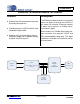
CDB5343 CDB5343: Evaluation Board for CS5343 Features Description Demonstrates Recommended Layout and Grounding Arrangements CS8406 Generates S/PDIF and EIAJ-340Compatible Digital Audio Requires Only an Analog Signal Source and Power Supply for a Complete Analogto-Digital Converter System The CDB5343 evaluation board is an excellent means for quickly evaluating the CS5343 24bit, stereo A/D converter. Evaluation requires a digital signal analyzer, an analog source, and a power supply.
CDB5343 TABLE OF CONTENTS 1. SYSTEM OVERVIEW ............................................................................................................................. 4 1.1 CS5343 ............................................................................................................................................. 4 2. CS8406 DIGITAL AUDIO TRANSMITTER ............................................................................................ 4 3. CRYSTAL OSCILLATOR ...............................
CDB5343 LIST OF FIGURES Figure 1. FFT (-1 dB 48 kHz) ...................................................................................................................... 9 Figure 2. FFT (-60 dB, 48 kHz) ................................................................................................................... 9 Figure 3. FFT (48 kHz, No Input) ................................................................................................................ 9 Figure 4. 48 kHz, THD+N vs. Input Freq ..
CDB5343 1. SYSTEM OVERVIEW The CDB5343 evaluation board is an excellent tool for evaluating the CS5343 Analog-to-Digital Converter (ADC). A minimum number of passive components condition the analog input signal prior to the CS5343, and the on-board CS8406 digital audio interface transmitter provides an easy interface to digital audio signal analyzers including the majority of digital audio test equipment. Additionally, the CDB5343 features an interface header (J3) for clock and data I/O.
CDB5343 The CS5343 generates sub-clocks when it is set for Master Mode via DIP switch S1. In this scenario, the CS8406 should be set to Slave Mode to receive sub-clocks. Similarly, the “SCLK, LRCK” switch should be closed to direct sub-clocks to the header. The sub-clock output of the J3 header is fixed at 3.3 V. If the user configures the CS5343 for Slave Mode, the device must receive sub-clocks either from the CS8406 or from an external source via header J3.
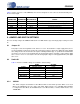
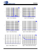
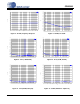
CDB5343 8. CONNECTORS Table 1 lists the connectors on the CDB5343, the reference designator of each connector, the directionality, and the associated signal.
CDB5343 Changing the state of this switch while the device is running will have no effect on the CS5343 as it must be reset to detect the change. Reset is accomplished by removing and restoring power to the device. Alternatively, removing and restoring MCLK will initiate a reset of the digital section, which is also sufficient for the CS5343 to detect a change in mode settings. 9.2.2 CS8406 This switch sets the CS8406 for either Master Mode or Slave Mode.
CDB5343 10.RESET The CS5343 features Power-On Reset which means that performing a full reset of the CS5343 requires a powercycling the device. On the CDB5343, this can be accomplished with by removing and restoring the power-supply or by removing and restoring the jumper on J3. Alternatively, removing and restoring MCLK to the device will effect a reset of just the digital portion of the device. The device enters Power-Down Mode when MCLK is removed and draws less current. 11.
CDB5343 12.PERFORMANCE PLOTS +0 +0 -10 -10 -20 -20 -30 -30 -40 -40 -50 d B F S -50 d B F S -60 -70 -60 -70 -80 -80 -90 -90 -100 -100 -110 -110 -120 -120 -130 20 50 100 200 500 1k 2k 5k 10k -130 20 20k 50 100 200 500 Hz 1k 2k 5k 10k 20k Hz Figure 1. FFT (-1 dB 48 kHz) Figure 2.
CDB5343 +5 +0 +4 -10 -20 +3 -30 +2 -40 -50 +1 d B F S d B +0 -1 -60 -70 -80 -2 -90 -100 -3 -110 -4 -120 -5 20 50 100 200 500 1k 2k 5k 10k -130 20 20k 50 100 200 500 Hz Figure 7. 48 kHz, Frequency Response +0 +0 -10 -10 -20 -20 -30 -30 -40 -40 5k 10k 20k -50 d B F S -60 -70 -60 -70 -80 -80 -90 -90 -100 -100 -110 -110 -120 -120 -130 20 2k Figure 8.
CDB5343 +40 +0 T TT T T TT T +35 -10 +30 +25 -20 +20 -30 +15 +10 -40 d B F S d B F S -50 -60 +5 +0 -5 -10 -70 -15 -20 -80 -25 -30 -90 -35 -100 -120 -100 -80 -60 -40 -20 -40 -140 +0 dBr -120 -100 -80 -60 -40 -20 +0 dBr Figure 13. 96 kHz, THD+N vs. Level Figure 14. 96 kHz, Fade-to-Noise Linearity +5 +0 -10 +4 -20 +3 -30 +2 -40 -50 +1 d B F S d B +0 -1 -60 -70 -80 -90 -2 -100 -3 -110 -4 -120 -5 20 50 100 200 500 1k 2k 5k 10k Hz Figure 15.
13.CDB PERFORMANCE CURVES 13.1 Total Harmonic Distortion + Noise (THD+N) Figure 17 shows typical THD+N performance of the CS5343 installed on the CDB5343. Performance curves are displayed for each channel with the CS5343 running at Single-Speed in both Master and Slave Modes and for VA voltages of both +3.3 V and 5 V. CDB5343 (Rev A device) THD+N vs.
DS687DB2 13.2 FFTlm Figure 18 shows a typical FFT of the output from the CS5343 on the CDB5343 with a 2 Vrms, 1 kHz sinewave input. For this plot, the device was configured for Single-Speed Mode with VA = 5 V.
DS687DB2 14.CDB SCHEMATICS Figure 19.
DS687DB2 CDB5343 15 Figure 20.
DS687DB2 CDB5343 16 Figure 21.
DS687DB2 CDB5343 17 Figure 22.
DS687DB2 CDB5343 18 Figure 23.
CDB5343 DS687DB2 Figure 24.
15.CDB LAYOUT CDB5343 DS687DB2 Figure 25.
DS687DB2 Figure 26.
Figure 27.
CDB5343 16.REVISION HISTORY Release Changes DB1 Initial Release DB2 Added Performance Plots Contacting Cirrus Logic Support For all product questions and inquiries, contact a Cirrus Logic Sales Representative. To find the one nearest you, go to www.cirrus.com. IMPORTANT NOTICE Cirrus Logic, Inc. and its subsidiaries ("Cirrus") believe that the information contained in this document is accurate and reliable.