
User Manual


DS899F1 23
CS4234
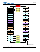
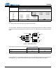
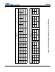
Figure 9. System Level Initialization and Power-up / Power-down Sequence
System
Operational
System
Unpowered
DAC1-4 Fully
Operational
ADC Data
Available on
SDOUT1
50 ms
Apply VL, VA, and MCLK
Clear PDN DACx & ADCx bits
Apply logic level high to Mute Pin
and RC network on Standby Pin
Clear MUTE_CHx bits
Start SCLK, FS/LRCK, SDINx
Write all required configuration
settings to Control Port
Clear reset to SMPS controller
Clear Mute DAC1-4 bits
Run Speaker Diagnostics by
setting the RUN DIAG bit
(if desired )
Ramp SMPS rails to +/- 4V
Write VA_SEL bit (in 0Fh)
appropr iately for VA
Clear Mute ADCx bits
Apply logic level low to Mute Pin
and RC network on Standby Pin
Ramp SMPS rails to +/- 4V
Set Mute ADCx bits
Set all PDN DAC & ADC bits
Stop SCLK, FS/LRCK, SDINx
Set VQ_RAMP bit
Remove VL, VA, and MCLK
Set Mute DAC1-4 bits
Set reset to SMPS controller
CS4234 Control
CS44417 Control
SMPS Control
CS4234 and CS44417 Control
Clear PDN_CHx bits
delay dependent
on RAM P _D IAG
pin capaci tor
delay dependent on
STBY pi n R C fil ter
delay dependent on
STBY pin RC filter
VQ Ready
(> 90% of Typical)
I
2
C Address
Captured & Control
Port Ready
250 m s
delay dependent
on DAC m ute /
unmute behavior
delay dependent
on DAC m ute /
unmute behavi or
2 ms + ( 3000/ M CLK)
2 ms +
(3000 /M CLK )
250 m s
DAC5 Fully
Operational
Clear Mute DAC5 (to SMPS)
delay dependent
on DAC mute/
unmute behavi or
Set Mute DAC5 (to SMPS)
delay dependent
on DAC m ute /
unmute behavi or
Set MUTE_CHx bits
Set PDN_CHx bits
Write all required configuration
settings to Control Port
Set RST
Set RST
Clear RST