
User Manual


DS899F1 32
CS4234
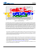
4.6 Internal Signal Path
The CS4234 device includes four main paths in which audio data can be routed. The analog input path,
shown in yellow, allows up to four analog signals to be combined into a single TDM stream on the SDOUT1
pin or output as stereo pairs on the SDOUT1 and SDOUT2 pins. The DAC1-4 path, highlighted in blue, con-
verts serial audio data to analog audio data. The DAC5 path is highlighted in red and can be used to create
a tracking power supply signal, to convert a digital tracking power supply signal to analog, or as a standard
audio CODEC with performance characteristics identical to the DACs found in the DAC1-4 path. Group de-
lay will often be added to the DAC1-4 path to allow the tracking power supply signal to lead the audio signal.
A low-latency path is provided as well to allow signals which should not be delayed to be mixed together
with the output signal at a point after the group delay block. The low-latency path is shown in green.
4.6.1 Routing the Serial Data within the Signal Paths
The serial port in the CS4234 is highly versatile and allows a number of ways that the serial data can be
coded into and extracted out of the TDM slots on the SDINx pins. Because of its versatility, it is possible
to errantly route the serial data into several of the available data paths. This mode of operation is not sup-
ported in the CS4234 and should not be used.
4.6.1.1 ADC Signal Routing
In TDM mode, the CS4234 is designed to load the first four slots of the TDM stream on the SDOUT1 pin
with the internal ADC data. Additionally, in order to minimize the number of SDOUT1 lines that must be
run to the system controller in a multiple IC application, the SDOUT1 data for up to 4 devices can be load-
ed into a single TDM stream by side chaining the devices together, as shown in Figure 20. To enable the
sidechain feature, the “SDO CHAIN” bit in the "SP Control" register must be set.
In Left Justified or I²S mode, the CS4234 transmits the AIN1 and AIN2 signals on the SDOUT1 pin and
the AIN3 and AIN4 signals on the SDOUT2 pin.
Gain / Volume
AIN4 (±)
AIN3 (±)
AIN2 (±)
AIN1 (±)
Inter polation
Filter
Channel Volum e ,
Mute, Invert ,
Noise Gate
Multi-bit
Modulators
AOUT1 (±)
AOUT2 (±)
AOUT3 (±)
AOUT4 (±)
I
2
C Control
Data
Control Port
Level T ransl ator
VL
1 .8 to 5. 0 VDC
RSTINT
SDIN1SDOUTx
Group
Delay
0-500 uS
Master C lock In
Fram e Sync
Cloc k / LRC K
SDIN 2
Serial Clock
In / Out
LDO Analog Supply
2.5 V
VA
5.0 VDC
VD
2. 5 VD C
Low -Latency
Demux
5
th
DAC
Input Advisory
DAC &
Anal og
Filters
Tracking
SMPS
Enabl e
Sample
& Hold
Mute , Invert ,
Noise Gate
Master
Volume
Control
TDM Serial Interface
AOUT 5 (±)
(SMPS C ontr ol )
DAC &
Anal og
Filters
Master
Vol . Cntrl
Select
Master Volume
0 dB
TPS
GAIN
Filter
Select
X
Inter polati on Fil ter
Sample & Hold
Max
Detect
Envelope
Trac ki ng
Mute, Invert ,
Noise Gate
DAC
Volume
Multi-bit
Modul ator s
Mode
Select
Full Scale C ode
DC Offset
X
Digital Filters
Multi-bit
ADC
-2
X
Gain
Select
-1
Figure 19. Audio Path Routing