
User Manual


DS851F2 11
CS42L56
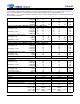
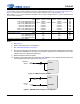
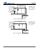
2. TYPICAL CONNECTION DIAGRAMS
Note 1
Note 2
2.2 µF
Note 1
Analog
Input 1
Analog
Input 2
1 µF
GND/Thermal Pad
VL
0.1 µF
+1.65 V to +3.63 V
RESET
R
p
LRCK
MCLK
SCLK
2.2 µF
+VHPFILT
VDFILT
LINEREF
SDIN
SDOUT
1 µF
AIN2REF
AIN1A
1800 pF
1800 pF
100 k
100
AIN1B
*
*
Digital Audio
Processor
AIN2A
1800 pF
1800 pF
AIN2B
*
*
FLYC
FLYN
-VHPFILT
2. 2 µ F
1 µ F
1 µF
1 µF
1 µF
100 k
100
100
100
100 k
100 k
2.2 µ F
**
**
VCP
AIN1REF
1 µ F
LINEOUTA
LINEOUTB
0.1 µF
VA
+1.65 V to +2.75 V
0.1 µF
VLDO
2.2 µ F
VQ
AGND
NPO /C0G dielectric capacitors.
1000 pF
AFILTA
AFILTB
1000 pF
2.2 µF
*
*
HPOUTB
HPOUTA
Headphone Out
Left & Right
33
0.1 µ F
HPDETECT
33
0.1 µ F
47 k
HPREF
FILT+
+1.65 V to +2.75 V
FLYP
2.2 µ F
**
**
**
Note 1
Notes:
1. The headphone amplifier’s output power and distortion are rated using the nominal capacitance shown. Larger capacitance
reduces the ripple on the internal amplifiers’ supplies and in turn reduces the amplifier’s distortion at high output power levels.
Smaller capacitance may not sufficiently reduce ripple to achieve the rated output power and distortion. Since the actual value
of typical X7R/X5R ceramic capacitors deviates from the nominal value by a percentage specified in the manufacturer’s data
sheet, capacitors should be selected based on the minimum output power and maximum distortion required.
2. The headphone amplifier’s output power and distortion are rated using the nominal capacitance shown and using the default
charge pump switching frequency. The required capacitance follows an inverse relationship with the charge pump’s switching
frequency. When increasing the switching frequency, the capacitance may decrease; when lowering the switching frequency,
the capacitance must increase. Since the actual value of typical X7R/X5R ceramic capacitors deviates from the nominal value
by a percentage specified in the manufacturer’s data sheet, capacitors should be selected based on the minimum output
power , maximum distortion and maximum charge pump switching frequency required.
3. Additional bulk capacitance may be added to improve PSRR at low frequencies.
4. These capacitors serve as a charge reservoir for the internal switched capacitor ADC modulators and should be placed as
close as possible to the inputs. They are only needed when the PGA (Programmable Gain Amplifier ) is bypassed.
Note 4
Note 3
R
p
*
**
Low ESR, X7R/X5R dielectric capacitors.
**
**
**
**
**
**
**
**
**
** **
**
**
**
562
562
3300 pF
R
ext
R
ext
LPF i s Optional
Line Level Out
Left & Right
3300 pF
*
*
SCL\CCLK
SDA\CDIN
AD0\CS
TSTN
TSTN
Figure 1. Typical Connection Diagram - Four Pseudo-Differential Analog Inputs
CS42L56
Notes:
1. The headphone amplifier’s output power and distortion are rated using the nominal capacitance shown. Larger capacitance reduces the ripple on the internal
amplifiers’ supplies and in turn reduces the amplifier’s distortion at high output power levels. Smaller capacitance may not sufficiently reduce ripple to achieve the
rated output power and distortion. Since the actual value of typical X7R/X5R ceramic capacitors deviates from the nominal value by a percentage specified in the
manufacturer’s data sheet, capacitors should be selected based on the minimum output power and maximum distortion required.
2. The headphone amplifier’s output power and distortion are rated using the nominal capacitance shown and using the default charge pump switching frequency.
The required capacitance follows an inverse relationship with the charge pump’s switching frequency. When increasing the switching frequency, the capacitance
may decrease; when lowering the switching frequency, the capacitance must increase. Since the actual value of typical X7R/X5R ceramic capacitors deviates
from the nominal value by a percentage specified in the manufacturer’s data sheet, capacitors should be selected based on the minimum output power, maximum
distortion and maximum charge pump switching frequency required.
3. Additional bulk capacitance may be added to improve PSRR at low frequencies.
4. These capacitors serve as a charge reservoir for the internal switched capacitor ADC modulators and should be placed as close as possible to the inputs. They
are only needed when the PGA (Programmable Gain Amplifier) is bypassed.