
User guide

DS803F3 19
CS4353
4.9 Recommended Power-up and Power-down Sequences
4.9.1 Power-up Sequences
4.9.1.1 External RESET Power-up Sequence
Follow the power-up sequence below if the external RESET pin is used:
1. Hold RESET
low while the power supplies are turned on.
The VA and VCP supplies should be applied prior to or simultaneously with the VL supply. If the VL
supply is applied before the VA and VCP supplies, a DC offset will occur on the analog outputs. The
offset level is bimodal: either approximately 0.7 V below the VL supply or approximately 50 mV. The
first case can only occur if the VL supply is greater than approximately 1.2 V. Either offset level is
removed when the VA and VCP supplies are applied.
2. Set the I²S
/LJ, 1_2VRMS, and DEM configuration pins to the desired state.
3. Provide the correct MCLK, LRCK, and SCLK signals locked to the appropriate frequencies as
discussed in Section 4.3.
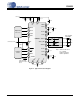
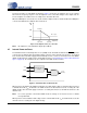
4. After the power supplies, configuration pins, and clock signals are stable, bring RESET
high. The
device will initiate the power-up sequence seen in Figure 9. The sequence will complete and audio
will be output from AOUTx within 50 ms after RESET
is set high.
4.9.1.2 Internal Power-on Reset Power-up Sequence
Follow the power-up sequence below if the internal power-on reset is used:
1. Hold RESET
high (connected to VL) while the power supplies are turned on.
The VA and VCP supplies should be applied prior to or simultaneously with the VL supply. If the VL
supply is applied before the VA and VCP supplies, a DC offset will occur on the analog outputs. The
offset level is bimodal: either approximately 0.7 V below the VL supply or approximately 50 mV. The
first case can only occur if the VL supply is greater than approximately 1.2 V. Either offset level is
removed when the VA and VCP supplies are applied.
The power-on reset circuitry will function as described in Section 4.7.
2. Set the I²S
/LJ, 1_2VRMS, and DEM configuration pins to the desired state.
3. After the power supplies and configuration pins are stable, provide the correct MCLK, LRCK, and
SCLK signals to progress from the ‘Power-Down State’ in the power-up sequence seen in Figure 9.
The sequence will complete and audio will be output from the AOUTx pins within 50 ms after valid
clocks are applied.
4.9.2 Power-down Sequences
4.9.2.1 External RESET
Power-down Sequence
Follow the power-down sequence below if the external RESET pin is used:
1. For minimal pops, set the input digital data to zero for at least 8192 consecutive samples.
2. Bring RESET
low.
3. Remove the power supply voltages.
4.9.2.2 Internal Power-on Reset Power-down Sequence
Follow the power-down sequence below if the internal power-on reset is used:
1. For minimal pops, set the input digital data to zero for at least 8192 consecutive samples.