
User Manual


Table Of Contents
- 1. Pin Description
- 2. Characteristics and Specifications
- Recommended Operating Conditions
- Absolute Maximum Ratings
- DAC Analog Characteristics
- Power and Thermal Characteristics
- Combined Interpolation & On-Chip Analog Filter Response
- Combined Interpolation & On-Chip Analog Filter Response
- DSD Combined Digital & On-Chip Analog Filter Response
- Digital Characteristics
- Switching Characteristics - PCM
- Switching Characteristics - DSD
- Switching Characteristics - Control Port - I·C Format
- Switching Characteristics - Control Port - SPI Format
- 3. Typical Connection Diagram
- 4. Applications
- 4.1 Master Clock
- 4.2 Mode Select
- 4.3 Digital Interface Formats
- Figure 8. Format 0 - Left-Justified up to 24-bit Data
- Figure 9. Format 1 - I·S up to 24-bit Data
- Figure 10. Format 2 - Right-Justified 16-bit Data
- Figure 11. Format 3 - Right-Justified 24-bit Data
- Figure 12. Format 4 - Right-Justified 20-bit Data
- Figure 13. Format 5 - Right-Justified 18-bit Data
- 4.3.1 OLM #1
- 4.3.2 OLM #2
- 4.4 Oversampling Modes
- 4.5 Interpolation Filter
- 4.6 De-Emphasis
- 4.7 ATAPI Specification
- 4.8 Direct Stream Digital (DSD) Mode
- 4.9 Grounding and Power Supply Arrangements
- 4.10 Analog Output and Filtering
- 4.11 The MUTEC Outputs
- 4.12 Recommended Power-Up Sequence
- 4.13 Recommended Procedure for Switching Operational Modes
- 4.14 Control Port Interface
- 4.15 Memory Address Pointer (MAP)
- 5. Register Quick Reference
- 6. Register Description
- 6.1 Chip Revision (Address 01h)
- 6.2 Mode Control 1 (Address 02h)
- 6.3 PCM Control (Address 03h)
- 6.4 DSD Control (Address 04h)
- 6.5 Filter Control (Address 05h)
- 6.6 Invert Control (Address 06h)
- 6.7 Group Control (Address 07h)
- 6.8 Ramp and Mute (Address 08h)
- 6.9 Mute Control (Address 09h)
- 6.10 Mixing Control (Address 0Ah, 0Dh, 10h, 13h)
- 6.11 Volume Control (Address 0Bh, 0Ch, 0Eh, 0Fh, 11h, 12h)
- 6.12 PCM Clock Mode (Address 16h)
- 7. Filter Response Plots
- Figure 24. Single-Speed (fast) Stopband Rejection
- Figure 25. Single-Speed (fast) Transition Band
- Figure 26. Single-Speed (fast) Transition Band (detail)
- Figure 27. Single-Speed (fast) Passband Ripple
- Figure 28. Single-Speed (slow) Stopband Rejection
- Figure 29. Single-Speed (slow) Transition Band
- Figure 30. Single-Speed (slow) Transition Band (detail)
- Figure 31. Single-Speed (slow) Passband Ripple
- Figure 32. Double-Speed (fast) Stopband Rejection
- Figure 33. Double-Speed (fast) Transition Band
- Figure 34. Double-Speed (fast) Transition Band (detail)
- Figure 35. Double-Speed (fast) Passband Ripple
- Figure 36. Double-Speed (slow) Stopband Rejection
- Figure 37. Double-Speed (slow) Transition Band
- Figure 38. Double-Speed (slow) Transition Band (detail)
- Figure 39. Double-Speed (slow) Passband Ripple
- Figure 40. Quad-Speed (fast) Stopband Rejection
- Figure 41. Quad-Speed (fast) Transition Band
- Figure 42. Quad-Speed (fast) Transition Band (detail)
- Figure 43. Quad-Speed (fast) Passband Ripple
- Figure 44. Quad-Speed (slow) Stopband Rejection
- Figure 45. Quad-Speed (slow) Transition Band
- Figure 46. Quad-Speed (slow) Transition Band (detail)
- Figure 47. Quad-Speed (slow) Passband Ripple
- 8. References
- 9. Parameter Definitions
- 10. Package Dimensions
- 11. Ordering Information
- 12. Revision History
DS619F1 35
CS4364
6.3.2 Functional Mode (FM)
Default = 11
00 - Single-Speed Mode (4 to 50 kHz sample rates)
01 - Double-Speed Mode (50 to 100 kHz sample rates)
10 - Quad-Speed Mode (100 to 200 kHz sample rates)
11 - Auto Speed Mode detect (32 kHz to 200 kHz sample rates)
Function:
Selects the required range of input sample rates or Auto Speed Mode.
6.4 DSD Control (Address 04h)
6.4.1 DSD Mode Digital Interface Format (DSD_DIF)
Default = 000 - Format 0 (64x oversampled DSD data with a 4x MCLK to DSD data rate)
Function:
The relationship between the oversampling ratio of the DSD audio data and the required Master clock to
DSD data rate is defined by the Digital Interface Format pins.
The DSD/PCM
bit determines whether PCM or DSD Mode is selected.
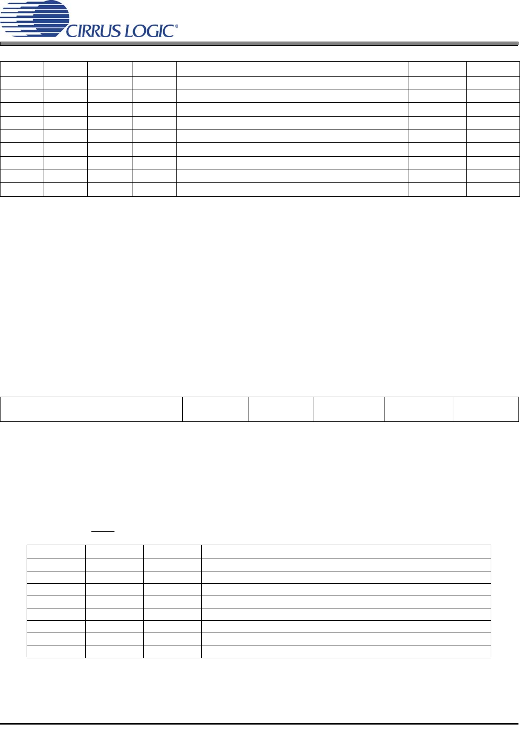
DIF3 DIF2 DIF1 DIF0 DESCRIPTION Format FIGURE
0000
Left Justified, up to 24-bit data
0 8
0001
I
2
S, up to 24-bit data
1 9
0010
Right Justified, 16-bit data
2 10
0011
Right Justified, 24-bit data
3 11
0100
Right Justified, 20-bit data
4 12
0101
Right Justified, 18-bit data
5 13
1000
One-line Mode 1, 24-bit Data
8 14
1001
One-line Mode 2, 20-bit Data
9 15
XXXX
All other combinations are Reserved
Table 7. Digital Interface Formats - PCM Mode
765 4 3 2 1 0
DSD_DIF2 DSD_DIF1 DSD_DIF0 DIR_DSD STATIC_DSD INVALID_DSD DSD_PM_MD DSD_PM_EN
000 0 1 1 0 0
DIF2 DIF1 DIFO DESCRIPTION
0 0 0 64x oversampled DSD data with a 4x MCLK to DSD data rate
0 0 1 64x oversampled DSD data with a 6x MCLK to DSD data rate
0 1 0 64x oversampled DSD data with a 8x MCLK to DSD data rate
0 1 1 64x oversampled DSD data with a 12x MCLK to DSD data rate
1 0 0 128x oversampled DSD data with a 2x MCLK to DSD data rate.
1 0 1 128x oversampled DSD data with a 3x MCLK to DSD data rate.
1 1 0 128x oversampled DSD data with a 4x MCLK to DSD data rate.
1 1 1 128x oversampled DSD data with a 6x MCLK to DSD data rate.
Table 8. Digital Interface Formats - DSD Mode