
User Manual
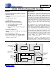


Table Of Contents
- 1. Pin Description
- 2. Characteristics and Specifications
- Recommended Operating Conditions
- Absolute Maximum Ratings
- DAC Analog Characteristics
- Power and Thermal Characteristics
- Combined Interpolation & On-Chip Analog Filter Response
- Combined Interpolation & On-Chip Analog Filter Response
- DSD Combined Digital & On-Chip Analog Filter Response
- Digital Characteristics
- Switching Characteristics - PCM
- Switching Characteristics - DSD
- Switching Characteristics - Control Port - I·C Format
- Switching Characteristics - Control Port - SPI Format
- 3. Typical Connection Diagram
- 4. Applications
- 4.1 Master Clock
- 4.2 Mode Select
- 4.3 Digital Interface Formats
- Figure 8. Format 0 - Left-Justified up to 24-bit Data
- Figure 9. Format 1 - I·S up to 24-bit Data
- Figure 10. Format 2 - Right-Justified 16-bit Data
- Figure 11. Format 3 - Right-Justified 24-bit Data
- Figure 12. Format 4 - Right-Justified 20-bit Data
- Figure 13. Format 5 - Right-Justified 18-bit Data
- 4.3.1 OLM #1
- 4.3.2 OLM #2
- 4.4 Oversampling Modes
- 4.5 Interpolation Filter
- 4.6 De-Emphasis
- 4.7 ATAPI Specification
- 4.8 Direct Stream Digital (DSD) Mode
- 4.9 Grounding and Power Supply Arrangements
- 4.10 Analog Output and Filtering
- 4.11 The MUTEC Outputs
- 4.12 Recommended Power-Up Sequence
- 4.13 Recommended Procedure for Switching Operational Modes
- 4.14 Control Port Interface
- 4.15 Memory Address Pointer (MAP)
- 5. Register Quick Reference
- 6. Register Description
- 6.1 Chip Revision (Address 01h)
- 6.2 Mode Control 1 (Address 02h)
- 6.3 PCM Control (Address 03h)
- 6.4 DSD Control (Address 04h)
- 6.5 Filter Control (Address 05h)
- 6.6 Invert Control (Address 06h)
- 6.7 Group Control (Address 07h)
- 6.8 Ramp and Mute (Address 08h)
- 6.9 Mute Control (Address 09h)
- 6.10 Mixing Control (Address 0Ah, 0Dh, 10h, 13h)
- 6.11 Volume Control (Address 0Bh, 0Ch, 0Eh, 0Fh, 11h, 12h)
- 6.12 PCM Clock Mode (Address 16h)
- 7. Filter Response Plots
- Figure 24. Single-Speed (fast) Stopband Rejection
- Figure 25. Single-Speed (fast) Transition Band
- Figure 26. Single-Speed (fast) Transition Band (detail)
- Figure 27. Single-Speed (fast) Passband Ripple
- Figure 28. Single-Speed (slow) Stopband Rejection
- Figure 29. Single-Speed (slow) Transition Band
- Figure 30. Single-Speed (slow) Transition Band (detail)
- Figure 31. Single-Speed (slow) Passband Ripple
- Figure 32. Double-Speed (fast) Stopband Rejection
- Figure 33. Double-Speed (fast) Transition Band
- Figure 34. Double-Speed (fast) Transition Band (detail)
- Figure 35. Double-Speed (fast) Passband Ripple
- Figure 36. Double-Speed (slow) Stopband Rejection
- Figure 37. Double-Speed (slow) Transition Band
- Figure 38. Double-Speed (slow) Transition Band (detail)
- Figure 39. Double-Speed (slow) Passband Ripple
- Figure 40. Quad-Speed (fast) Stopband Rejection
- Figure 41. Quad-Speed (fast) Transition Band
- Figure 42. Quad-Speed (fast) Transition Band (detail)
- Figure 43. Quad-Speed (fast) Passband Ripple
- Figure 44. Quad-Speed (slow) Stopband Rejection
- Figure 45. Quad-Speed (slow) Transition Band
- Figure 46. Quad-Speed (slow) Transition Band (detail)
- Figure 47. Quad-Speed (slow) Passband Ripple
- 8. References
- 9. Parameter Definitions
- 10. Package Dimensions
- 11. Ordering Information
- 12. Revision History
DS619F1 7
CS4364
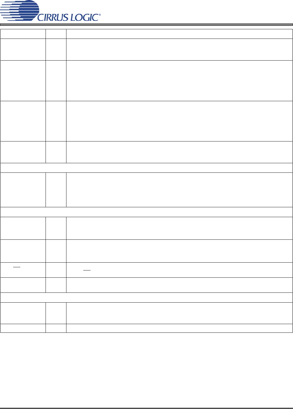
FILT+ 20
Positive Voltage Reference (Output) - Positive reference voltage for the internal sampling cir-
cuits. Requires the capacitive decoupling to analog ground as shown in the Typical Connection
Diagram.
AOUT1
AOUT2
AOUT3
AOUT4
AOUT5
AOUT6
39
38
35
34
29
28
Analog Output (Output) - The full scale analog output level is specified in the Analog Character-
istics specification table.
MUTEC1
MUTEC2
MUTEC3
MUTEC4
MUTEC5
MUTEC6
41
26
25
24
23
22
Mute Control (Output) - These pins are intended to be used as a control for external mute circuits
on the line outputs to prevent the clicks and pops that can occur in any single supply system.
TST_OUT
40, 37
36, 33
30, 27
Test Output - These pins need to be floating and not connected to any trace or plane.
Hardware Mode Definitions
M0
M1
M2
M3
M4
17
16
15
12
10
Mode Selection (Input) - Determines the operational mode of the device as detailed in Tables 4
and 5.
Software Mode Definitions
SCL/CCLK 15
Serial Control Port Clock (Input) - Serial clock for the serial control port. Requires an external
pull-up resistor to the logic interface voltage in I²C
®
mode as shown in the Typical Connection Dia-
gram.
SDA/CDIN 16
Serial Control Port Data (Input/Output) - SDA is a data I/O line in I²C mode and is open drain,
requiring an external pull-up resistor to the logic interface voltage, as shown in the Typical Con-
nection Diagram; CDIN is the input data line for the control port interface in SPI
™
mode.
AD0/CS
17
Address Bit 0 (I²C) / Control Port Chip Select (SPI) (Input) - AD0 is a chip address pin in I²C
mode; CS
is the chip select signal for SPI mode.
TST
10
12
Test - These pins need to be tied to analog ground.
DSD Definitions
DSD1, DSD2
DSD3, DSD4
DSD5, DSD6
3, 2
1, 48
47,46
Direct Stream Digital Input (Input) - Input for Direct Stream Digital serial audio data.
DSD_SCLK 42 DSD Serial Clock (Input) - Serial clock for the Direct Stream Digital serial audio interface.
Pin Name # Pin Description