
Instruction Manual

DS723F1 9
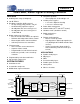
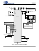
CS43L21
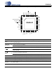
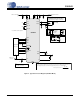
2. TYPICAL CONNECTION DIAGRAMS
1 µF
+1.8 V or +2.5 V
1 µF
VQ
FILT+
0.1 µF
1 µF
DGND
VL
0.1 µF
+1.8 V, +2.5 V
or +3.3 V
SCL/CCLK
SDA/CDIN
RESET
2 k
See Note 1
LRCK
AGND
AD0/CS
MCLK
SCLK
0.1 µF
VA_HP
VD
SDIN
CS43L21
2 k
1 µF
+1.8 V or +2.5 V
AOUTB
AOUTA
470
470
C
C
R
ext
R
ext
See Note 2
Note 1:
Resistors are required for I²C
control port operation
For best response to Fs/2 :
4704
470
ext
ext
RFs
R
C
This circuitry is intended for applications where the
CS43L21 connects directly to an unbalanced output of the
device. For internal routing applications please see the
DAC Analog Output Characteristics section for loading
limitations.
Note 2 :
Digital Audio
Processor
0.1 µF
VA
Headphone Out
Left & Right
Line Level Out
Left & Right
Speaker Driver
FLYP
FLYN
VSS_HP
GND_HP
1 µF
51.1
0.022 µF
1 µF
**
**
* *Use low ESR ceramic capacitors.
See Note 3
Note 3:
Series resistance in the path of the power supplies must
be avoided. Any voltage drop on VA_HP will directly
impact the negative charge pump supply (VSS_HP) and
result in clipping on the audio output .
1.5 µF
1.5 µF
See Note 4
Note 4 :
Larger capacitors, such as 1.5 µF, improves the charge
pump performance (and subsequent THD+N) at the full
scale output power achieved with gain (G) settings
greater than default.
**
**
Figure 1. Typical Connection Diagram (Software Mode)