
Instruction Manual

DS632F1 17
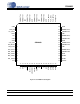
CS44800
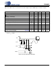
PS_SYNC 3
Power Supply Synchronization Clock (Output) - The PWM synchronized clock to the
switch mode power supply.
XTI 5
Crystal Oscillator Input (Input) - Crystal Oscillator input or accepts an external clock
input signal that is used to drive the internal PWM core logic.
XTO 6 Crystal Oscillator Output (Output) - Crystal Oscillator output.
SYS_CLK 8
External System Clock (Output) - Clock output. This pin provides a divided down clock
derived from the XTI input.
DAI_MCLK 9 Digital Audio Input Master Clock (Input) - Master audio clock.
DAI_SCLK 10
Digital Audio Input Serial Clock (Input) - Serial clock for the Digital Audio Input Inter-
face. The clock frequency is a multiple of the Left/Right Clock running at Fs.
DAI_LRCK 11
Digital Audio Input Left/Right Clock (Input) - Determines which channel, Left or Right,
is currently active on the serial audio data line. The rate is determined by the sampling fre-
quency Fs.
DAI_SDIN1
DAI_SDIN2
DAI_SDIN3
DAI_SDIN4
12
13
14
15
Digital Audio Input Serial Data (Input) - Input for two’s complement serial audio data.
MUTE 20
Mute (Input) - The device will perform a hard mute on all channels. All internal registers
are not reset to their default settings.
SCL/CCLK 21
Serial Control Port Clock (Input) - Serial clock for the serial control port. Requires an
external pull-up resistor to the logic interface voltage in I²C mode as shown in the Typical
Connection Diagram.
SDA/CDOUT 22
Serial Control Data (Input/Output) - SDA is a data I/O line in I²C mode and requires an
external pull-up resistor to the logic interface voltage, as shown in the Typical Connection
Diagram.; CDOUT is the output data line for the control port interface in SPI mode.
AD1/CDIN 23
Address Bit 1 (I²C)/Serial Control Data (SPI) (Input) - AD1 is a chip address pin in I²C
mode.;CDIN is the input data line for the control port interface in SPI mode.
AD0/CS
24
Address Bit 0 (I²C)/Control Port Chip Select (SPI) (Input) - AD0 is a chip address pin in
I²C mode; CS
is the chip select signal in SPI mode.
INT 25
Interrupt Request (Output) - CMOS or open-drain interrupt request output. This pin is
driven to the configured active state to indicate that the PWM Controller has status data
that should be read by the host.
RST 26
Reset (Input) - The device enters a low power mode and all internal registers are reset to
their default settings when low.
GPIO6 29
General Purpose Input, Output (Input/Output) - This pin is configured as an input follow-
ing a RST
condition. It can be configured as a general purpose input or output which can
be individually controlled by the Host Controller.
GPIO5 30
General Purpose Input, Output (Input/Output) - This pin is configured as an input follow-
ing a RST
condition. It can be configured as a general purpose input or output which can
be individually controlled by the Host Controller.
GPIO4 31
General Purpose Input, Output (Input/Output) - This pin is configured as an input follow-
ing a RST
condition. It can be configured as a general purpose input or output which can
be individually controlled by the Host Controller.
GPIO3 32
General Purpose Input, Output (Input/Output) - This pin is configured as an input follow-
ing a RST
condition. It can be configured as a general purpose input or output which can
be individually controlled by the Host Controller.