
User`s manual


Operational Mode Selection
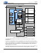
CS485xxr Hardware User’s Manual
DS734UM7 Copyright 2009 Cirrus Logic, Inc. 2-2
2.2 Operational Mode Selection
The operational mode for the CS485xx is selected by the values of the HS[4:0] pins on the rising edge of
RESET
. This value determines the communication mode used until the part is reset again. This value also
determines the method for loading application code. The table below shows the different operational modes
and the HS[4:0] values for each mode.
2.3 Slave Boot Procedures
When the CS485xx is the slave boot device, the system host controller (as the master boot device) must
follow an outlined procedure for correctly loading application code. The slave boot procedure is described in
this section. Slave boot requires the system host controller to send messages to, and read back messages
from, the
CS485xx. These messages have been outlined in Section 2.3.3 "Boot Messages" on page 2-6.
The
CS485xx has different.uld files (overlays) for certain processing tasks. Slave booting the CS485xx
requires loading multiple overlays - differing from previous Cirrus Logic Audio DSP families (that is,
CS493xx, CS494xxx). Please refer to AN298, “
CS485xx Firmware User’s Manual” regarding more
information on the breakdown of processing tasks for each overlay.
Table 2-1. Operation Modes
HS[4:0] Mode
Boot Master
Device
Boot Slave Device
X0000
Master I
2
C
a
a. In I
2
C master mode, the Image Start address (0x0) is sent as a 16-bit value, with the default I
2
C
address of 0x50, I
2
C clock frequency = F
dclk
/ 72.
CS485xx
I
2
C External ROM
X1000
Master SPI 1
b
b. SPI master mode 1 is to support the legacy 16-bit SPI EEPROM. The following defaults are used: SPI
Command Byte 0x03, Image Start address 0x0 is sent as a 16-bit value, no dummy bytes, SPI clock
frequency = F
dclk
/ 4.
CS485xx
SPI (Mode 1) External ROM
5, 6, 7
X0001
Master SPI 2
c
c. In SPI Master mode 2, the following defaults are used: SPI Command Byte 0x68, Image Start address
0x0 is sent as a 24-bit value, 4 dummy bytes sent following the address (and before reading image
data), SPI clock frequency = Fdclk / 2. This mode supports the Atmel
®
SPI Flash memory.
CS485xx
SPI (Mode 2) External ROM
5, 6, 7
X1001
Master SPI 3
d
d. In SPI Master mode 3, the following defaults are used: SPI command byte 0x03, Image Start address
0x0 is sent as a 24-bit value, no dummy bytes, SPI clock frequency = F
dclk
/ 2. This mode supports the
ST SPI EEPROM devices.
CS485xx
SPI (Mode 3) External ROM
e, f,g
e. For all SPI Master boot modes, by default GPIO13 is used as EE_CS.
f. For Flash Master modes, the following defaults are used: clock ratio=1:1, Endian Mode = little-endian,
Chip Select polarity = active-low, 0-cycle delay from CS Address Change to Output Enable, 4-cycle
delay from CS to Read Access.
g. F
dclk
is specified in the CS485xx Data Sheet.
X 0 0 1 0 RESERVED
X 1 0 1 0 RESERVED
XX10 0
Slave I
2
C
System Host CS485xx
X X 1 0 1 Slave SPI System Host CS485xx
X X 1 1 0 RESERVED
X X 1 1 1 RESERVED
X X 0 1 1 RESERVED