
Owner's manual

DS868PP2 Copyright 2008 Cirrus Logic, Inc. 3
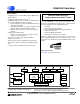
CS49DV8C Data Sheet
32-bit Audio DSP Family
Table of Contents
1. Documentation Strategy .................................................................................................................5
2. Overview ..........................................................................................................................................5
2.1 Licensing .........................................................................................................................................................7
3. Firmware Supported .......................................................................................................................7
4. Hardware Functional Description .................................................................................................7
4.1 DSP Core ........................................................................................................................................................7
4.1.1 DSP Memory ......................................................................................................................................7
4.1.2 DMA Controller ...................................................................................................................................7
4.2 On-chip DSP Peripherals ................................................................................................................................8
4.2.1 Digital Audio Input Port (DAI) ..............................................................................................................8
4.2.2 Digital Audio Output Port (DAO) .........................................................................................................8
4.2.3 Serial Control Port 1 & 2 (I
2
C
®
or SPI
™
) ............................................................................................8
4.2.4 External Memory Interface .................................................................................................................8
4.2.5 GPIO ...................................................................................................................................................8
4.2.6 PLL-based Clock Generator ...............................................................................................................8
4.3 DSP I/O Description ........................................................................................................................................9
4.3.1 Multiplexed Pins .................................................................................................................................9
4.3.2 Termination Requirements ..................................................................................................................9
4.3.3 Pads ...................................................................................................................................................9
4.4 Application Code Security ...............................................................................................................................9
5. Characteristics and Specifications .............................................................................................10
5.1 Absolute Maximum Ratings ...........................................................................................................................10
5.2 Recommended Operating Conditions ...........................................................................................................10
5.3 Digital DC Characteristics .............................................................................................................................10
5.4 Power Supply Characteristics ....................................................................................................................... 11
5.5 Thermal Data (128-Pin LQFP) ...................................................................................................................... 11
5.6 Switching Characteristics— RESET ..............................................................................................................12
5.7 Switching Characteristics — XTI ...................................................................................................................13
5.8 Switching Characteristics — Internal Clock ...................................................................................................13
5.9 Switching Characteristics — Serial Control Port - SPI Slave Mode ..............................................................14
5.10 Switching Characteristics — Serial Control Port - SPI Master Mode ..........................................................15
5.11 Switching Characteristics — Serial Control Port - I
2
C Slave Mode .............................................................16
5.12 Switching Characteristics — Serial Control Port - I
2
C Master Mode ...........................................................17
5.13 Switching Characteristics — UART .............................................................................................................18
5.14 Switching Characteristics — Digital Audio Slave Input Port ........................................................................19
5.15 Switching Characteristics — Digital Audio Output Port ...............................................................................20
5.16 Switching Characteristics — SDRAM Interface ...........................................................................................22
6. Ordering Information ....................................................................................................................27
7. Environmental, Manufacturing, and Handling Information ......................................................27
8. Device Pin-Out Diagram ...............................................................................................................28
8.1 128-Pin LQFP Pin-Out Diagram.................................................................................................................... 28
9. Package Mechanical Drawings ....................................................................................................29
9.1 128-Pin LQFP Package .................................................................................................................................29
10. Revision History ..........................................................................................................................30