
User Manual

4 DS625F5
CS5364
5.3 01h (GCTL) Global Mode Control Register ...................................................................................32
5.4 02h (OVFL) Overflow Status Register ........................................................................................... 33
5.5 03h (OVFM) Overflow Mask Register ............................................................................................ 33
5.6 04h (HPF) High-Pass Filter Register ............................................................................................. 34
5.7 05h Reserved ................................................................................................................................ 34
5.8 06h (PDN) Power Down Register .................................................................................................. 34
5.9 07h Reserved ................................................................................................................................ 34
5.10 08h (MUTE) Mute Control Register .............................................................................................. 34
5.11 09h Reserved .............................................................................................................................. 35
5.12 0Ah (SDEN) SDOUT Enable Control Register ............................................................................ 35
6. FILTER PLOTS ..................................................................................................................................... 36
7. PARAMETER DEFINITIONS ................................................................................................................ 39
8. PACKAGE DIMENSIONS ................................................................................................................... 40
THERMAL CHARACTERISTICS .......................................................................................................40
9. ORDERING INFORMATION ................................................................................................................ 41
10. REVISION HISTORY ......................................................................................................................... 41
LIST OF FIGURES
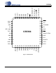
Figure 1. CS5364 Pinout ............................................................................................................................. 6
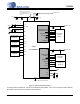
Figure 2. Typical Connection Diagram ........................................................................................................ 9
Figure 3. I²S/LJ Timing .............................................................................................................................. 15
Figure 4. TDM Timing ............................................................................................................................... 16
Figure 5. I²C Timing .................................................................................................................................. 17
Figure 6. SPI Timing ................................................................................................................................. 18
Figure 7. Crystal Oscillator Topology ........................................................................................................ 20
Figure 8. Master/Slave Clock Flow ........................................................................................................... 21
Figure 9. Master and Slave Clocking for a Multi-Channel Application ...................................................... 21
Figure 10. I²S Format ................................................................................................................................ 22
Figure 11. LJ Format ................................................................................................................................. 22
Figure 12. TDM Format ............................................................................................................................. 23
Figure 13. Master Mode Clock Dividers .................................................................................................... 24
Figure 14. Slave Mode Auto-Detect Speed ............................................................................................... 24
Figure 15. Recommended Analog Input Buffer ......................................................................................... 28
Figure 16. SPI Format ............................................................................................................................... 30
Figure 17. I²C Write Format ...................................................................................................................... 31
Figure 18. I²C Read Format ...................................................................................................................... 31
Figure 19. SSM Passband ........................................................................................................................ 36
Figure 20. DSM Passband ........................................................................................................................ 36
Figure 21. QSM Passband ........................................................................................................................ 36
Figure 22. SSM Stopband ......................................................................................................................... 37
Figure 23. DSM Stopband ......................................................................................................................... 37
Figure 24. QSM Stopband ........................................................................................................................ 37
Figure 25. SSM -1 dB Cutoff ..................................................................................................................... 38
Figure 26. DSM -1 dB Cutoff .................................................................................................................... 38
Figure 27. QSM -1 dB Cutoff ..................................................................................................................... 38