
Technical data


24
DESIGN NOTE
Quad SPI Flash: A Simpler, Faster Alternative to Standard SPI Flash
When Adding External Memory to 32-bit MCU Systems
By: Frederik De Swaef, Field Applications Engineer, Macronix and Francesco Petruzziello, MCU Product Application Engineer, NXP
The modern 32-bit microcontroller is a
remarkably capable device, but its abilities
have given rise to a problem for the design
engineers who use them; faced with ever-
growing demand for more features, such as
more detailed graphics or a greater range of
languages to be supported in the user inter-
face, designers are finding themselves limited
by the small size of the typical MCU’s on-chip
Flash memory.
Today, 32-bit MCUs are normally supplied with
an on-chip Flash memory no larger than 1Mb.
And the options for extending this on-board
memory have changed in recent years; it is now
rare to add external parallel Flash, since few
MCUs support the parallel external memory
interface. One of the reasons for this lack of
support is the number of pins a parallel Flash
needs for a 8- or 16-bit data bus and 20 or more
address and control lines.
SPI NOR Flash is another option that the design
could consider, but this memory type is much
slower than on-chip and parallel Flash. Further,
it is normally impossible to execute code from
SPI Flash; even if it is possible, the performance
is poor.
To solve this problem of adding external Flash
memory, NXP Semiconductors has developed
a new, easy-to-use external memory interface.
Called SPI Flash Interface (SPIFI), it is intended
for use with the popular Quad SPI NOR Flash
memory type, which is cost effective and
provides a wide choice of densities.
SPIFI is available today in the LPC1800 family of
ARM
®
Cortex
®
-M3 MCUs from NXP, and in the
LPC4000 and LPC4300 families of ARM Cortex-
M4MCUs. (SPIFI support will be added to more
NXP MCUs, in future). SPIFI support means that
these controllers can benefit from the proven
Quad SPI memory technology provided by the
MX25 range of Serial NOR Flash devices from
Macronix. These range in size from 8Mb to
512Mb, and are suitable for both fast data
storage and in-place code execution.
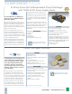
Quad SPI is a modified serial peripheral interface
which is capable of communicating on four data
lines; traditional SPI uses only a single line. This
multiplies the data throughput by almost four
times, and makes high-performance execution in
place possible. Compared to parallel NOR Flash
with a 16-bit data bus, Quad SPI NOR Flash can
achieve almost twice the total throughput (see
Figure 1).
Figure 1: Quad SPI NOR Flash offers throughput nearly two
times greater than that of parallel NOR Flash
Throughput is not Quad SPI’s only advantage;
requiring only six connections between the MCU
and the memory IC, routing is far less complex
than that of a parallel Flash design, which calls
for between 30 and 45 tracks.
Macronix Quad SPI Flash choices
The MX25 series of Quad SPI Flash memories
from Macronix is available in various small
8- and 16-pin packages. These SOP, WSON and
USON devices have a very small board footprint.
Macronix has taken care to give various MX25
devices of different memory densities the same
footprint or a compatible footprint, so that OEMs
can migrate from one density to another without
making any changes to board layout. Only when
migrating to a density higher than 128Mb does
the designer have to implement minor software
changes to support 4-byte addressing.
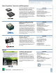
In NXP MCUs, the SPIFI interface is directly
connected to the ARM core’s AMBA High
performance Bus (AHB), which means that the
Quad SPI Flash is mapped and accessible for
transfer via I/O or DMA channels (see Figure 2).
When executing in place, instructions are loaded
into the SPIFI buffers directly from the external
Flash, with no software overhead.
The Quad SPI Flash itself is controlled by five
registers. These registers set the configuration
and commands for reading and retrieving status
information, and are transparently used by the
on-chip ROM driver and the SPIFI library. They
can also be directly accessed by the user
application if desired.
Figure 2: The Quad SPI Flash memory is directly connected to
the AHB via SPIFI
The MCU’s SPIFI hardware controls the process
for reading from the Quad SPI Flash. If code is
stored there, the hardware will fetch it automati-
cally in accordance with the register settings,
with no software intervention. Initiation of
writing and erasing operations is controlled by
software settings.
The commands for data transfer have the same
structure as those of a conventional SPI Flash
memory; they specify the command, address and
data for reading and writing (see Figure 3). With
Quad SPI Flash, the command will be sent on
one line, and the address on four lines. Data are
also moved from Flash on four lines. The use of
four lines means that sending a 24-bit or 3-byte
address requires only six clock cycles, instead
of 24 in an SPI Flash memory. Similarly, 1 byte of
data is received in two clock cycles instead
of eight.
1.800.FUTURE.1 • www.FutureElectronics.com