
Technical data


25
DESIGN NOTE
To buy products or download data, go to
www.FutureElectronics.com/FTM
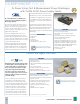
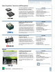
Figure 3: The Quad SPI Flash command structure is similar to
that of conventional SPI Flash
The Macronix MX25 Flash memories are capable
of running at a clock frequency up to 104MHz
during all operations. For read operations, the
designer must take into account the need for
dummy cycles after transferring the address
when calculating the access time required
to fetch the first byte. After the first byte, the
address will automatically be incremented and
data will be sent out with no additional access
time until the Select pin goes high again. This
enables a fast data throughput when reading
sequential data.
Random read operations, such as branching in
instructions, must use the Enhanced Read mode.
This mode enables data to be read without
sending a Read command. The address alone
needs to be provided, saving eight clock cycles.
The Enhanced Read mode is set by toggling bits
in the dummy cycles of the first read operation.
All subsequent reads only need to transmit the
address.
NXP MCUs’ Support for Quad SPI Flash
Some NXP ARM Cortex-M MCUs have no on-
chip Flash memory. This includes the LPC1810,
LPC1820, LPC1830 and LPC1850, and also the
LPC4310, LPC4320, LPC4330, LPC4350 and
LPC4370. All these devices, however, can use
external Quad SPI Flash as their sole non-volatile
memory for data and code storage and for in-
place execution, enjoying outstanding read and
write performance.
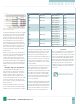
The Macronix MX25Lxxx35E/F series is ideal
for this, offering densities from 8Mb to 512Mb
(64MB) in 8-pin or 16-pin packages (see Table 1).
The designer has the flexibility to migrate during
development without being tied to one density,
while benefiting from high performance com-
bined with a very low bill of materials cost.
SPIFI is also implemented in LPC MCUs which do
feature on-chip Flash. In this case, the function
of the Quad SPI external Flash is to extend the
on-chip memory, providing extra code- or data-
storage capability.
This is often required in graphical user interfaces
(GUIs). Traditionally in these applications, the
image data are stored in an external SPI or
parallel Flash, with the disadvantages described
above. Data often need to be shifted from the
external device into internal or external RAM,
and then moved again to the display itself. This
means that the data have to be moved twice
before being displayed.
The high throughput of the MX25 Quad SPI Flash
and the memory-mapped SPIFI interface allow
data to be shifted directly from external Flash to
the display. Now, the data are moved only once
and the amount of RAM needed as well as the
memory bus load can be markedly reduced.
Density MXIC type Part number Package
8Mb MX25L8035E MX25L8035EM2I-10G 8-SOP
16Mb MX25L1635E MX25L1636EM2I-08G 8-SOP
32Mb MX25L3235E
MX25L3235EMI-10G 16-SOP
MX25L3235EM2I-10G 8-SOP
MX25L3235EZNI-10G 8-WSON
64Mb MX25L6435E
MX25L6435EMI-10G 16-SOP
MX25L6435EM2I-10G 8-SOP
MX25L6435EZNI-10G 8-WSON
MX25L6435EZ2I-10G 8-WSON
128Mb MX25L12835F
MX25L12835FM2I-10G 8-SOP
MX25L12835FMI-10G 16-SOP
MX25L12835FZ2I-10G 8-WSON
MX25L12835FZNI-10G 8-WSON
256Mb MX25L25635F
MX25L25635FMI-10G 16-SOP
MX25L25635FZ2I-10G 8-WSON
512Mb MX25L51235F
MX66L51235FMI-10G 16-SOP
MX66L51235FZ2I-10G 8-WSON
Conclusion
When a 32-bit MCU has no on-chip Flash memory,
or its on-board Flash is not large enough, the
ideal solution is to add a Quad SPI external Flash
memory. Quad SPI Flash supported by the SPIFI
interface implemented in NXP ARM Cortex-M
MCUs removes the complexity of designing with
external parallel Flash, reducing pin count and
offering better performance. This makes the
combination a good choice for many applications
in industrial equipment, consumer devices and
white goods.
Table 1: Macronix offers a broad choice of Quad SPI NOR Flash memories
1.800.FUTURE.1 • www.FutureElectronics.com