
Technical Specs

Version:
1.01
Department:
IoT
Last Modification:
2016-12-13
Author:
Kamil Chwałek
5
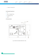
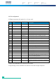
1.6. Pin assignment
21 Edge connectors with pads 0.6 x 0.6 mm each.
Pin
Name
Pin function
Description
1
Vbatt
Power
Power supply 1.8-3.6 V
2
GND
Ground
Should be connected to ground plane on application
PCB
3
PIO 0 / UART TX
Digital I/O
General purpose I/O pin or UART TX line
4
PIO 1 / UART RX
Digital I/O
General purpose I/O pin or UART RX line
5
PIO 3
Digital I/O
General purpose I/O line
6
PIO 4
Digital I/O
General purpose I/O line
7
PIO 6
Digital I/O
General purpose I/O pin or DEBUG_CS# line*
8
PIO 7
Digital I/O
General purpose I/O pin or DEBUG_MOSI line*
9
PIO 8
Digital I/O
General purpose I/O pin or DEBUG_MISO line*
10
PIO 9
Digital I/O
General purpose I/O line
11
PIO 5
Digital I/O
General purpose I/O pin or DEBUG_CLK line*
12
PIO 10
Digital I/O
General purpose I/O line
13
SPIPIO#
Input pin
Selects SPI debug on PIO[8:5] line*
14
PIO 2 / I2C_P
Output pin
EEPROM power supply line
15
PIO 11
Digital I/O
General purpose I/O line
16
AIO 0
ADC input 0
Analogue programmable I/O line
17
AIO 1
ADC input 1
Analogue programmable I/O line
18
AIO 2
ADC input 2
Analogue programmable I/O line
19
WAKE
External wake
Input to wake from hibernate or dormant mode If not
in use, pin should be grounded
20
I2C_SDA
I2C data pin
I2C data input / output line
21
I2C_SCL
I2C clock pin
I2C clock line
22
GND
Ground
Should be connected to ground plane on application
PCB
All pins are compatible with CSR1012 chip pinout.
*Programming is also available from bottom PCB side through testpoints.