CMX-ZG03 Datasheet (VER.0.
Data Sheet : CMX-ZG03 ZigBee 3.0 , ZigBee PRO and IEEE802.15.4 Module Overview CMX-ZG03은 using the IEEE802.15.4 standard in the 2.4 GHz - 2.5 GHz ISM frequency band, including ZigBee 3.0 and ZigBee PRO stack with Home Automation, Light Link and Smart Energy profiles. The modules integrate all of the RF components required, removing the need to perform expensive RF design and test. Products can be designed by simply connecting sensors and switches to the module IO pins.
Benefits • • • • Microminiature module solutions Ready to use in products Minimises product development time No RF test required for systems Applications • • • • • Robust and secure low-power wireless applications ZigBee Smart Energy networks ZigBee Home Automation networks Toys and gaming peripherals Energy harvesting - for example, self-powered light switch Features: Module • 2.4GHz IEEE 802.15.4, , ZigBee 3.
Contents 1. Introduction ……………………………………………………………………………………5 1.1. Variants…………………………………………………………………………………………………….. 5 2. Specifications………………………………………………………………………………….6 3. Product Development………………………………………………………………………...7 3.1. JN5XXX Single Chip Wireless Microcontroller……………..……………………….…………….…….7 4. Pin Configurations………………………………………………………….………….…..…8 4.1. Pin Assignment……………………………………………………………………………………..….…. 9 4.2. Pin Descriptions………………………………..……………………………………………………...… 12 4.2.1 Power Supplies…………………………………..
1. Introduction CMX-ZG03 is a range of ultra-low power, high performance surface mount modules targeted at IEEE 802.15.4, ZigBee 3.0 and ZigBee Home Automation, Light Link and Smart Energy networking applications, enabling users to realize products with minimum time to market and at the lowest cost. They remove the need for expensive and lengthy development of custom RF board designs and test suites.
2. Specifications VDD=3.0V @ +25°C Typical DC Characteristics Notes CMX-ZG03 Deep sleep current 70nA Sleep current Radio transmit current Radio receive current 0.73uA In sleep mode; with I/O and RC oscillator timer wake-up; 25mA 10dBm @2.8V 17.8mA Centre frequency accuracy +/-25ppm Maximu input level at 10dBm Additional +/-15ppm allowance for temperature and ageing Typical RF Characteristics Receive sensitivity -96dBm Transmit power Maximum input signal 10dBm 22dBm 9.
Programmable analogue comparators 1 Internal temperature sensor and battery monitor 1 Ultra low power mode for sleep 3. Product Development A range of evaluation/developer kits is also available, allowing products to be quickly bread boarded. Efficient development of software applications is enabled by the provision of a complete, unlimited, software developer kit. Together with the available libraries for the IEEE802.15.
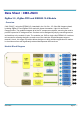
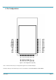
4. Pin Configurations Figure 1: Pin Configuration (top view) Note : that the same basic pin configuration applies for all module designs. However, DIO2 (pin 8) and DIO3 (pin 9) are not available on the RZN-AEM00 and RZN-AEM05.
4.1.
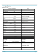
Symbol Pin Type[1] Description DIO7/RXD0/JTAG_TDI/PWM3 13 DIO7 — DIO7 I/O RXD0 — UART 0 receive data input JTAG_TDI — JTAG data input PWM3 — PWM 3 data output DIO8/TIM0CK_GT/PC1/PWM4 14 I/O DIO8 — DIO8 TIM0CK_GT — timer0 clock/gate input PC1 — pulse counter1 input PWM4 — PWM 4 output DIO9/TIM0CAP/32KXTALIN/RXD1/32KIN 15 I/O DIO9 — DIO9 TIM0CAP — Timer0 Capture input 32KXTALIN — 32 kHz External Crystal input RXD1 — UART1 Receive Data input 32KIN — 32 kHz External clock input DIO10/TIM0OUT/32KX
Symbol Pin Type[1] Description DIO15[8] 24 DIO15 — DIO15 I/O SIF_D — serial interface data RXD0 — UART 0 receive data input RXD1 — UART 1 receive data input JTAG_TDI — JTAG data input SPISEL2 — SPI-bus master select output 2 SPISCLK — SPI-bus slave clock input DIO16/SPISMOSI/SIF_CLK/COMP1P 25 I/O DIO16 — DIO16 COMP1P — comparator positive input SIF_CLK — Serial Interface clock SPISMOSI — SPI-bus Slave Master Out Slave In input DIO17/SPISMISO/SIF_D/COMP1M 26 I/O DIO17 — DIO17 COMP1M — COMP1M; c
4.2. Pin Descriptions 4.2.1. Power Supplies A single power supply pin, VDD is provided.. 5. Electrical Characteristics In most cases, the Electrical Characteristics are the same for both module and chip. They are described in detail in the chip datasheet. Where there are differences, they are detailed below. 5.1. Maximum Ratings Exceeding these conditions will result in damage to the device. Parameter Min Max Device supply voltage VDD -0.3V 3.6V All Pins -0.3V VDD + 0.
6.
Appendix A Additional Information A.1.
A.2.
FCC Infformation to User as been tested and fo und to com or a Class B digital This equipment ha mply with the limits fo device, pursuant to Part 15 of the FCC Rules. Thesse limits are designed to provide reasona able protecction againsst harmful i nterference in a residential insta llation.
ot be co-located or op erated in CAUTIO ON : This device and its antenna (s) must no odify this conjuncction with any other antenna or transmitter. End serss cannot mo d the user’s authority to transmiitter device. Any una thorized m odification could void operate e this device. mited to ins tallation in fixed appl ications, and only installed Door Lock System This mo odule is lim This module can not be attached to other device without Door Lock System device.