
User Manual

MRFE6VP61K25HR6 MRFE6VP61K25HSR6
1
RF Device Data
Freescale Semiconductor
RF Power Field Effect Transistors
High Ruggedness N--Channel
Enhancement--Mode Lateral MOSFETs
These high ruggedness devices are designed for use in high VSWR industrial
(including laser and plasma exciters), broadcast (analog and digital), aerospace
and radio/land mobile applications. They are unmatched input and output
designs allowing wide frequency range utilization, between 1.8 and 600 MHz.
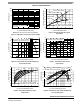
! Typical Performance: V
DD
=50Volts,I
DQ
= 100 mA
Signal Type
P
out
(W)
f
(MHz)
G
ps
(dB)
"
D
(%)
IRL
(dB)
Pulsed (100 #sec,
20% Duty Cycle)
1250 Peak 230 24.0 74.0 -- 1 4
CW 1250 CW 230 22.9 74.6 -- 1 5
! Capable of Handling a Load Mismatch of 65:1 VSWR, @ 50 Vdc,
230 MHz, at all Phase Angles, Designed for Enhanced Ruggedness,
1250 Watts Pulsed Peak Power, 20% Duty Cycle, 100 μ sec
! Capable of 1250 Watts CW Operation
Features
! Unmatched Input and Output Allowing Wide Frequency Range Utilization
! Device can be used Single--Ended or in a Push--Pull Configuration
! Qualified Up to a Maximum of 50 V
DD
Operation
! Characterized from 30 V to 50 V for Extended Power Range
! Suitable for Linear Application with Appropriate Biasing
! Integrated ESD Protection with Greater Negative Gate--Source Voltage
Range for Improved Class C Operation
! Characterized with Series Equivalent Large--Signal Impedance Parameters
! RoHS Compliant
! In Tape and Reel. R6 Suffix = 150 Units, 56 mm Tape Width, 13 inch Reel.
For R5 Tape and Reel options, see p. 12.
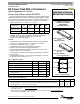
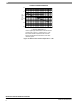
Table 1. Maximum Ratings
Rating Symbol Value Unit
Drain--Source Voltage V
DSS
--0.5, +125 Vdc
Gate--Source Voltage V
GS
--6.0, +10 Vdc
Storage Temperature Range T
stg
-- 65 to +150 $C
Case Operating Temperature T
C
150 $C
Total Device Dissipation @ T
C
=25$C
Derate above 25 $C
P
D
1333
6.67
W
W/$C
Operating Junction Temperature
(1,2)
T
J
225 $C
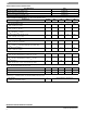
Table 2. Thermal Characteristics
Characteristic Symbol Value
(2,3)
Unit
Thermal Resistance, Junction to Case
Case Temperature 66$C, 1250 W Pulsed, 100 #sec Pulse Width, 20% Duty Cycle, 100 mA, 230 MHz
Case Temperature 63$C, 1250 W CW, 100 mA, 230 MHz
Z
%
JC
R
%
JC
0.03
0.15
$C/W
1. Continuous use at maximum temperature will affect MTTF.
2. MTTF calculator available at http://www.freescale.com/rf
. Select Software & Tools/Development Tools/Calculators to access MTTF
calculators by product.
3. Refer to AN1955, Thermal Measurement Methodology of RF Power Amplifiers. Go to http://www.freescale.com/rf
.
Select Documentation/Application Notes -- AN1955.
Document Number: MRFE6VP61K25H
Rev. 1, 1/2011
Freescale Semiconductor
Technical Data
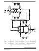
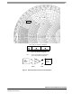
1.8--600 MHz, 1250 W CW, 50 V
LATERAL N--CHANNEL
BROADBAND
RF POWER MOSFETs
MRFE6VP61K25HR6
MRFE6VP61K25HSR6
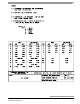
(Top View)
RF
out
/V
DS
31
Figure 1. Pin Connections
42
RF
out
/V
DS
RF
in
/V
GS
RF
in
/V
GS
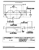
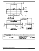
CASE 375D--05, STYLE 1
NI--1230
MRFE6VP61K25HR6
CASE 375E--04, STYLE 1
NI--1230S
MRFE6VP61K25HSR6
PARTS ARE PUSH--PULL
& Freescale Semiconductor, Inc., 2010--2011.
A
ll rights reserved.