
User Manual


PNP RF Transistor
This device is designed for general RF amplifier and mixer
applications to 250 mHz with collector currents in the 1.0 mA
to 30 mA range. Sourced from Process 75.
MMBTH81MPSH81
Absolute Maximum Ratings* TA = 25°C unless otherwise noted
*These ratings are limiting values above which the serviceability of any semiconductor device may be impaired.
Symbol Parameter Value Units
V
CEO
Collector-Emitter Voltage 20 V
V
CBO
Collector-Base Voltage 20 V
V
EBO
Emitter-Base Voltage 3.0 V
I
C
Collector Current - Continuous 50 mA
T
J
, T
stg
Operating and Storage Junction Temperature Range -55 to +150
°
C
Thermal Characteristics TA = 25°C unless otherwise noted
Symbol Characteristic Max Units
MPSH81 *MMBTH81
P
D
Total Device Dissipation
Derate above 25
°
C
350
2.8
225
1.8
mW
mW/
°
C
R
θ
JC
Thermal Resistance, Junction to Case 125
°
C/W
R
θ
JA
Thermal Resistance, Junction to Ambient 357 556
°
C/W
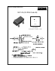
C
E
B
TO-92
C
B
E
SOT-23
Mark: 3D
*Device mounted on FR-4 PCB 1.6" X 1.6" X 0.06."
1997 Fairchild Semiconductor Corporation
NOTES:
1) These ratings are based on a maximum junction temperature of 150 degrees C.
2) These are steady state limits. The factory should be consulted on applications involving pulsed or low duty cycle operations.
3) All voltages (V) and currents (A) are negative polarity for PNP transistors.
MPSH81 / MMBTH81