USBS6 V 0.3 June 29, 2010 User Manual C1030-5510 SPARTAN-6TM FPGA board with USB2.0, SPI-Flash and JTAG interface. Order number: C1030-5510 USBS6 / C1030-5510 User Doc V0.3 http://www.cesys.
Copyright information Copyright © 2010 CESYS GmbH. All Rights Reserved. The information in this document is proprietary to CESYS GmbH. No part of this document may be reproduced in any form or by any means or used to make derivative work (such as translation, transformation or adaptation) without written permission from CESYS GmbH.
Overview Summary of USBS6 USBS6 is a low-cost multilayer PCB with SPARTAN-6TM FPGA and USB 2.0 Interface. 34 I/O balls of the FPGA are available on standard 2.54mm headers, 81 I/O balls can be reached through a industry standard VG 96-pin connector. It offers multiple configuration options including USB and onboard SPI-Flash and can also be used standalone without the need of a USB interface. Feature list Form factor XILINX SPARTAN-6TM USB2.
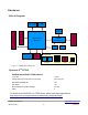
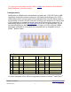
Hardware Block Diagram 128Mb QSPI Flash 64kb I²C EEPROM XILINX FPGA Spartan-6 USB2.
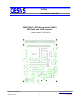
Figure 2: USBS6 Top View USBS6 / C1030-5510 User Doc V0.3 http://www.cesys.
Powering USBS6 USBS6 may be used bus-powered (see SW2 below) without the need of any external power supply other than USB. In this mode VCCO_IO on J3,PIN A3, B3, C3 sourcing capability is limited due to the fact, that USB power supply current is limited depending on which system is used as host. Typically USB hosts allow up to 500mA. In bus-powered mode, at first only FX2 is enabled. After successful connection to the operating system the further power-on sequencing behavior depends on UDK configuration.
! It is strongly recommended to check XILINXTM UG381 about Spartan-6 FPGA SelectIO Signal Standards on XILINXTM website. Configuration Configuration of USBS6 can be accomplished in several ways: JTAG, SPI-Flash or USB. The default configuration mode is booting from SPI-Flash. After powering on the FPGA, USBS6 always tries to configure itself from the attached Flash using SPI Master mode. If no valid design is stored in the SPI-Flash the FPGA has to be configured via JTAG or USB.
FPGA the reader is encouraged to take a look at the user guide UG380 on XILINXTM web page. USB2.0 controller CYPRESSTM FX2LPTM is a highly integrated, low power USB2.0 microcontroller, that integrates USB2.0 transceiver, serial interface engine (SIE), enhanced 8051 microcontroller and a programmable peripheral interface. More information on usage of FX2LP TM in conjunction with Spartan-6 can be found in chapter C. USB2.
USB2.0 FX2LPTM Microcontroller CYPRESSTM CY7C68013A Signal Name FPGA IO FX2_FD11 U13 FX2_FD12 V13 FX2_FD13 U10 FX2_FD14 R8 FX2_FD15 T8 Comment External memory USBS6 offers the opportunity to use various external memory architectures in one´s FPGA design. With Micron Technology MT46H64M16LFCK-5 up to 1Gbit of high-speed lowpower DDR SDRAM is available.
LPDDR SDRAM MT46H64M16LFCK-5 Signal Name FPGA IO MCB1_RAS_n K15 MCB1_CAS_n K16 MCB1_WE_n K12 MCB1_CS_n -- MCB1_CKE_n D17 Clock enable: CKE HIGH activates, and CKE LOW deactivates, the internal clock signals, input buffers, and output drivers. Taking CKE LOW enables PRECHARGE power-down and SELF REFRESH operations (all banks idle), or ACTIVE power-down (row active in any bank). CKE is synchronous for all functions except SELF REFRESH exit.
LPDDR SDRAM MT46H64M16LFCK-5 Signal Name FPGA IO MCB1_DQ12 T17 MCB1_DQ13 T18 MCB1_DQ14 U17 MCB1_DQ15 U18 MCB1_UDQS N15 Comment Data strobe for Upper Byte Data bus: Output with read data, input with write data. DQS is edge-aligned with read data, center-aligned in write data. It is used to capture data. * As the memory device interface of Spartan-6 supports only one device, CS# signal is not supported by Spartan-6 MCB. CS# is pulled LOW via an external 0 Ohm resistor.
configurable LEDs allow to make internal monitoring status signals visible by driving the appropriate FPGA IO to a HIGH level. Figure 4: Bitte durch Orginalbild ersetzen LEDs Signal Name FPGA IO Comment SYS_LED0 -- Internal 5V power supply. SYS_LED1 -- Power OK- signal from onboard voltage regulator. SYS_LED2 V17 Illuminates to indicate the status of the DONE pin if FPGA is successfully configured. USER_LED0 P7 User- configurable LED. USER_LED1 N7 User- configurable LED.
HEX rotary DIP switch DIAL FPGA Pin N8 FPGA Pin M11 FPGA Pin M10 FPGA Pin N9 5 0 1 0 1 6 1 0 0 1 7 0 0 0 1 8 1 1 1 0 9 0 1 1 0 A 1 0 1 0 B 0 0 1 0 C 1 1 0 0 D 0 1 0 0 E 1 0 0 0 F 0 0 0 0 FT232R from FTDI is a USB to serial UART interface. USB to serial UART interface Signal Name FPGA IO Direction Comment FTDI_TXD U15 FPGA IN Transmit asynchronous data output for FT232R. FTDI_RXD V15 FPGA OUT Receiving asynchronous data input for FT232R.
Figure 5: VG 96-pin external expansion connector J3 J3 VG 96-pin external expansion connector PIN FPGA IO Comment PIN FPGA IO Comment PIN FPGA IO Comment A32 -- GND B32 -- GND C32 -- GND A31 F13 VG96_IO78 B31 E13 VG96_IO79 C31 C4 VG96_IO80 A30 F12 VG96_IO75 B30 E12 VG96_IO76 C30 F11 VG96_IO77 A29 D11 VG96_IO72* B29 C11 VG96_IO73* C29 E11 VG96_IO74 A28 G11 VG96_IO69 B28 F10 VG96_IO70 C28 G8 VG96_IO71 A27 G9 VG96_IO66 B27 F9 VG96_IO67 C27 F8 VG96_IO6
J3 VG 96-pin external expansion connector PIN FPGA IO Comment PIN FPGA IO A7 N2 VG96_IO9 B7 N1 A6 P2 VG96_IO6 B6 A5 T2 VG96_IO3 A4 U2 A3 Comment PIN FPGA IO Comment VG96_IO10 C7 N4 VG96_IO11 P1 VG96_IO7 C6 N3 VG96_IO8 B5 T1 VG96_IO4 C5 P4 VG96_IO5 VG96_IO0 B4 U1 VG96_IO1 C4 P3 VG96_IO2 -- VCCO_IO B3 -- VCCO_IO C3 -- VCCO_IO A2 -- GND B2 -- GND C2 -- GND A1 -- 5.0V_EXT B1 -- 5.0V_EXT C1 -- 5.
J4 IDC 2x25-Pin external expansion connector PIN FPGA IO Comment PIN FPGA IO Comment 25 B11 ADD_IO16 26 A11 ADD_IO17 27 B12 ADD_IO18 28 A12 ADD_IO19 29 B14 ADD_IO20 30 A14 ADD_IO21 31 B16 ADD_IO22 32 A16 ADD_IO23 33 -- GND 34 -- GND 35 C10 ADD_IO24* 36 A10 ADD_IO25* 37 D12 ADD_IO26 38 C12 ADD_IO27 39 -- GND 40 -- GND 41 C13 ADD_IO28 42 A13 ADD_IO29 43 D14 ADD_IO30 44 C14 ADD_IO31 45 C15 ADD_IO32 46 A15 ADD_IO33 47 D4 HSWAPEN** 48 --
FPGA design Cypress FX-2 LP and USB basics Several data transfer types are defined in USB 2.0 specification. High-speed bulk transfer is the one and only mode of interest to end users. USB transfers are packet oriented and have a time framing scheme. USB packets consist of USB protocol and user payload data. Payload could have a variable length of up to 512 bytes per packet.
In FPGA designs with multiple clock domains asynchronous FIFOs have to be used for transferring data from one clock domain to the other and comprehensive control signals have to be resynchronized. Other clock sources can be added internally by using Spartan-6 TM onchip digital clock managers (DCMs) or PLLs or externally by connecting clock sources to other FPGA global clock inputs. A wide range of clock frequencies can be synthesized with DCMs and PLLs.
VHDL. Verilog and schematic entry design flows are not supported. • The design “usbs6_soc” demonstrates the implementation of a system-on-chip (SoC) with host software access to the peripherals like GPIOs, external Flash Memory, LPDDR Memory and internal BlockRAM over USB. This design requires a protocol layer over the simple USB bulk transfer (see CESYS application note “Transfer Protocol for CESYS USB products” for details), which is already provided by CESYS software API.
After ProgramFPGA() is called and the FPGA design is completely downloaded, the pin #RESET (note: the prefix # means, that the signal is active low) is automatically pulsed (HIGH/LOW/HIGH). This signal can be used for resetting the FPGA design. The APIfunction ResetFPGA() can be called to initiate a pulse on #RESET at a user given time.
HARDWARE-CIRCUITS OR ANY OTHER KIND OF ASIC OR PROGRAMMABLE LOGIC DESIGN), EVEN IF THE COPYRIGHT HOLDER HAS BEEN ADVISED OF THE POSSIBILITY OF SUCH DAMAGES. Design “usbs6_soc” An on-chip-bus system is implemented in this design. The VHDL source code shows you, how to build a 32 Bit WISHBONE based shared bus architecture. All devices of the WISHBONE system support only SINGLE READ / WRITE Cycles. Files and modules having something to do with the WISHBONE system are labeled with the prefix “wb_”.
(BFM), too. These can be used for behavioral simulation purposes. src/usbs6_soc_top.vhd: This is the top level entity of the design. The WISHBONE components are instantiated here. src/wb_intercon.vhd: All WISHBONE devices are connected to this shared bus interconnection logic. Some MSBs of the address are used to select the appropriate slave. src/wb_ma_fx2.vhd: This is the entity of the WISHBONE master, which converts the CESYS USB protocol into one or more 32 Bit single read/write WISHBONE cycles.
programming FPGA configuration bitstream to SPI-FLASH and the other accesses QUADSPI-FLASH for storing nonvolatile application data. src/wb_sl_mcb.vhd: WISHBONE adapter for one port of Spartan-6TM build in multiport memory controller block (MCB). src/wb_sl_uart.vhd: This entity is a simple UART transceiver with 16 byte buffer for each direction connected to USB2UART interface. XilinxTM UART transceiver macros are used as physical layer.
app_fifo_wr_data_i D0 D1 D2 D3 D4 124 125 126 D3 D2 D1 3 2 1 app_fifo_wr_full_o app_fifo_wr_count_o 122 123 127 ifclk app_fifo_rd_i D4 app_fifo_rd_data_o D0 app_fifo_rd_empty_o app_fifo_rd_count_o 5 4 0 FPGA => FX-2 app_fifo_wr_i FX-2 => FPGA ifclk Figure 9: FIFO transactions of fx2_slfifo_ctrl at user logic side The upper waveform demonstrates the behavior of app_fifo_wr_full_o and app_fifo_wr_count_o when there is no transaction on the slave FIFO controller side of the FIFO.
src/sync_fifo.vhd: This entity is a general purpose synchronous FIFO buffer. It is build of FPGA distributed RAM. src/sfifo_hd_a1Kx18b0K5x36.vhd: This entity is a general purpose synchronous FIFO buffer with mismatched port widths. It is build of a FPGA BlockRAM. src/flash_ctrl.vhd: The low level FLASH controller for SPI FLASH memory. It supports reading and writing of four bytes of data at one time as well as erasing the whole memory. usbs6_soc.xise: Project file for XilinxTM ISE usbs6_soc.
incremented automatically in block transfers. You can find details on enabling/disabling the burst mode and address auto-increment mode in the CESYS application note “Transfer Protocol for CESYS USB products” and software API documentation. CESYS USB transfer protocol is converted into one or more WISHBONE data transaction cycles. So the FX-2 becomes a master device in the internal WISHBONE architecture. Input signals for the WISHBONE master are labeled with the postfix “_I”, output signals with “_O”.
Basic WISHBONE cycle CLK STB WE ADR32 Master DAT32M DAT32S Slave ACK Figure 10: WISHBONE transactions with WriteRegister() WriteBlock() ReadRegister() ReadBlock() The WISHBONE signals in these illustrations and explanations are shown as simple bit types or bit vector types, but in the VHDL code these signals could be encapsulated in extended data types like arrays or records. Example: ... port map ( ... ACK_I => intercon.masters.slave(2).ack, ...
WISHBONE cycles. It is a reduced version of “usbs6_soc” example implementing a single BlockRAM slave. Files and modules src/wishbone_pkg.vhd: See chapter “Design usbs6_soc” src/usbs6_bram_top.vhd: This is the top level module. It instantiates FX-2 module as a WISHBONE master device (wb_ma_fx2.vhd) and a BlockRAM as a WISHBONE slave device (wb_sl_bram.vhd). src/wb_ma_fx2.vhd: See chapter “Design usbs6_soc” src/wb_sl_bram.vhd: See chapter “Design usbs6_soc” src/sim_tb/wb_sl_bram_tb.
wb_sl_bram_tb.cmd: Win32 batch file automatically starting ModelSim with example testbench and appropriate simulation script (wb_sl_bram_tb.do). Just doubleclick for running the demo! USBS6 / C1030-5510 User Doc V0.3 http://www.cesys.
Software Introduction The UDK (Unified Development Kit) is used to allow developers to communicate with Cesys's USB and PCI(e) devices. Older releases were just a release of USB and PCI drivers plus API combined with some shared code components. The latest UDK combines all components into one single C++ project and offers interfaces to C++, C and for .NET (Windows only).
Windows Requirements To use the UDK in own projects, the following is required: • • • • Installed drivers Microsoft Visual Studio 2005 or 2008; 2010 is experimental CMake 2.6 or higher ⇒ http://www.cmake.org wxWidgets 2.8.10 or higher (must be build separately) ⇒ http://www.wxwidgets.org [optionally, only if UDKLab should be build] Driver installation The driver installation is part of the UDK installation but can run standalone on final customer machines without the need to install the UDK itself.
lets assume to use c:\\udkapi. c: cd \udkapi CMake allows the build directory separated to the source directory, so it's a good idea to do it inside an empty sub-directory: mkdir build cd build The following code requires an installation of CMake and at least one supported Visual Studio version. If CMake isn't included into the PATH environment variable, the path must be specified as well: cmake .. This searches the preferred Visual Studio installation and creates projects for it.
Linux There are too many distributions and releases to offer a unique way to the UDK installation. We've chosen to work with the most recent Ubuntu release, 9.10 at the moment. All commands are tested on an up to date installation and may need some tweaking on other systems / versions. Requirements • • • • GNU C++ compiler toolchain zlib development libraries CMake 2.6 or higher ⇒ http://www.cmake.org wxWidgets 2.8.10 or higher ⇒ http://www.wxwidgets.
following command has to be done: sudo make install This will do the following things: • Install the kernel module inside the module library path, update module dependencies • Install a new udev rule to give device nodes the correct access rights (0666) (/etc/udev/rules.d/99-ceusbuni.rules) • Install module configuration file (/etc/dev/modprobe.d/ceusbuni.conf) • Start module If things work as intended, there must be an entry /proc/ceusbuni after this procedure.
Build drivers: cd PlxSdk/Linux/Driver PLX_SDK_DIR=`pwd`/../../ ./buildalldrivers Loading the driver manually requires a successful build, it is done using the following commands: cd ~/udkapi2.
the application that uses it. Otherwise unwanted side effects in exception handling will occur ! (See example in Add project to UDK build). USBS6 / C1030-5510 User Doc V0.3 http://www.cesys.
Use APIs in own projects C++ API • Include file: udkapi.h • Library file: • Windows: udkapi_vc[ver]_[arch].lib, [ver] is 8, 9, 10, [arch] is x86 or amd64, resides in lib/[build]/ • Linux: libusbapi.so, resides in lib/ • Namespace: ceUDK As this API uses exceptions for error handling, it is really important to use the same compiler and build settings which are used to build the API itself. Otherwise exception based stack unwinding may cause undefined side effects which are really hard to fix.
.NET API • Include file: • Library file: udkapinet.dll, resided in bin/[build] • Namespace: cesys.ceUDK The .NET API, as well as it example application is separated from the normal UDK build. First of all, CMake doesn't have native support .NET, as well as it is working on Windows systems only. Building it has no dependency to the standard UDKAPI, all required sources are part of the .NET API project. The Visual Studio solution is located in directory dotnet/ inside the UDK installation root.
Methods/Functions GetLastErrorCode API C++ C .NET Code unsigned int ceException::GetErrorCode() unsigned int GetLastErrorCode() uint ceException.GetLastErrorCode() Returns an error code which is intended to group the error into different kinds. It can be one of the following constants: Error code Kind of error ceE_TIMEOUT ceE_IO_ERROR ceE_UNEXP_HW_BEH ceE_PARAM ceE_RESOURCE ceE_API ceE_ORDER ceE_PROCESSING ceE_INCOMPATIBLE ceE_OUTOFMEMORY Errors with any kind of timeout.
Device enumeration The complete device handling is done by the API internally. It manages the resources of all enumerated devices and offers either a device pointer or handle to API users. Calling Init() prepares the API itself, while DeInit() does a complete cleanup and invalidates all device pointers and handles. To find supported devices and work with them, Enumerate() must be called after Init().
Enumerate API C++ C .NET Code static void ceDevice::Enumerate(ceDevice::ceDeviceType DeviceType) CE_RESULT Enumerate(unsigned int DeviceType) static void ceDevice.Enumerate(ceDevice.ceDeviceType DeviceType) Search for (newly plugged) devices of the given type and add them to the internal list. Access to this list is given by GetDeviceCount() / GetDevice().
GetDevice API C++ C .NET Code static ceDevice *ceDevice::GetDevice(unsigned int uiIdx) CE_RESULT GetDevice(unsigned int uiIdx, CE_DEVICE_HANDLE *pHandle) static ceDevice ceDevice.GetDevice(uint uiIdx) Get device pointer or handle to the device with the given index, which must be smaller than the device count returned by GetDeviceCount(). This pointer or handle is valid up to the point DeInit() is called. USBS6 / C1030-5510 User Doc V0.3 http://www.cesys.
Information gathering The functions in this chapter return valuable information. All except GetUDKVersionString() are bound to devices and can be used after getting a device pointer or handle from GetDevice() only. Methods/Functions GetUDKVersionString API C++ C .NET Code static const char *ceDevice::GetUDKVersionString() const char *GetUDKVersionString() static string ceDevice.GetUDKVersionString() Return string which contains the UDK version in printable format. GetDeviceUID API C++ C .
Return device type name of given device pointer or handle. Notice C API: pszDest is the buffer were the value is stored to, it must be at least of size uiDestSize. GetBusType API C++ C .NET Code ceDevice::ceBusType ceDevice::GetBusType() CE_RESULT GetBusType(CE_DEVICE_HANDLE Handle, unsigned int *puiBusType) ceDevice.ceBusType ceDevice.GetBusType() Return type of bus a device is bound to, can be any of the following: Constant Bus ceBT_PCI ceBT_USB PCI bus USB bus GetMaxTransferSize API C++ C .
Using devices After getting a device pointer or handle, devices can be used. Before transferring data to or from devices, or catching interrupts (PCI), devices must be accessed, which is done by calling Open(). All calls in this section require an open device, which must be freed by calling Close() after usage. Either way, after calling Open(), the device is ready for communication. As of the fact, that Cesys devices usually have an FPGA on the device side of the bus, the FPGA must be made ready for usage.
Finish working with the given device. ReadRegister API Code C++ C .NET unsigned int ceDevice::ReadRegister(unsiged int uiRegister) CE_RESULT ReadRegister(CE_DEVICE_HANDLE Handle, unsigned int uiRegister, unsigned int *puiValue) uint ceDevice.ReadRegister(uint uiRegister) Read 32 bit value from FPGA design address space (internally just calling ReadBlock() with size = 4). WriteRegister API Code C++ C .
.NET unsigned char *pucData, unsigned int uiSize, unsigned int uiIncAddress) void ceDevice.WriteBlock(uint uiAddess, byte[] Data, uint uiLen, bool bIncAddress) Transfer a given block of data to the 32 bit bus system address uiAddress. The size should never exceed the value retrieved by GetMaxTransferSize() for the specific device. bIncAddress is at the moment available for USB devices only. It flags to write all data to the same address instead of starting at it. WaitForInterrupt API C++ C .
Pulses the FPGA reset line for a short time. This should be used to sync the FPGA design with the host side peripherals. ProgramFPGAFromBIN API Code C++ C .NET void ceDevice::ProgramFPGAFromBIN(const char *pszFileName) CE_RESULT ProgramFPGAFromBIN(CE_DEVICE_HANDLE Handle, const char *pszFileName) void ceDevice.ProgramFPGAFromBIN(string sFileName) Program the FPGA with the Xilinx tools .bin file indicated by the filename parameter. Calls ResetFPGA() subsequently. ProgramFPGAFromMemory API Code C++ C .
Set the timeout in milliseconds for data transfers. If a transfer is not completed inside this timeframe, the API generates a timeout error. EnableBurst API C++ C .NET Code void ceDevice::EnableBurst(bool bEnable) CE_RESULT EnableBurst(CE_DEVICE_HANDLE Handle, unsigned int uiEnable) void ceDevice.EnableBurst(bool bEnable) (PCI only) Enable bursting in transfer, which frees the shared address / data bus between PCI(e) chip and FPGA by putting addresses on the bus frequently only.
UDKLab Introduction UDKLab is a replacement of the former cesys-Monitor, as well as cesys-Lab and fpgaconv. It is primary targeted to support FPGA designers by offering the possibility to read and write values from and to an active design. It can further be used to write designs onto the device's flash, so FPGA designs can load without host intervention. Additionally, designs can be converted to C/C++ and C# arrays, which allows design embedding into an application. USBS6 / C1030-5510 User Doc V0.
The main screen The following screen shows an active session with an EFM01 device. The base view is intended to work with a device, while additional functionality can be found in the tools menu. The left part of the screen contains the device initialization details, needed to prepare the FPGA with a design (or just a reset if loaded from flash), plus optional register writes for preparation of peripheral components.
Using UDKLab After starting UDKLab, most of the UI components are disabled. They will be enabled at the point they make sense.
After a device has been selected, most UI components are available: • • • • FPGA configuration FPGA design flashing [if device has support] Project controls Initializer controls (Related to projects) The last disabled component at this point is the content panel. It is enabled if the initialization sequence has been run.
FPGA design flashing This option stores a design into the flash component on devices that have support for it. The design is loaded to the FPGA after device power on without host intervention. How and under which circumstances this is done can be found in the hardware description of the corresponding device. The following screen shows the required actions for flashing: Figure 14: Flash design to device Projects Device communication is placed into a small project management.
projects can be created. Only one project can be active in one session. Initializing sequence The initializing sequence is a list of actions that must be executed in order to work with the FPGA on the device.
• Download design from host • Load design from flash (supported on EFM01, USBV4F and USBS6) So the first entry in the initialize list must be a program entry or, if loaded from flash, a reset entry (To sync communication to the host side). Subsequent to this, a mix of register write and sleep commands can be placed, which totally depends on the underlying FPGA design. This can be a sequence of commands sent to a peripheral component or to fill data structures with predefined values.
Sequence start The button sitting below the list runs all actions from top to bottom. In addition to this, the remaining UI components, the content panel, will be enabled, as UDKLab expects a working communication at this point. The sequence can be modified an started as often as wished. Content panel The content panel can be a visual representation of the FPGA design loaded during initialization. It consists of a list of registers and data areas, which can be visit and modified using UDKLab.
Register entry A register entry can be used to communicate with a 32 bit register inside the FPGA. In UDKLab, a register consists of the following values: • Address • Name • Info text The visual representation of one register can be seen in the following image: Figure 18: Register panel The left buttons are responsible for adding new entries, move the entry up or down and removing the current entry, all are self explanatory. The header shows it's mapping name as well as the 32 bit address.
Data area entry A data area entry can be used to communicate with a data block inside the FPGA, examples are RAM or flash areas. Data can be transfered from and to files, as well as displayed in a live view. An entry constits of the following data: • • • • • Address Name Data alignment Size Read-only flag The visual representation is shown below. Figure 19: Data area panel Similar to the register visualization, the buttons on the right side can be used to add, move and remove data area panels.
Additional information Using SPI-Flash for configuration How to store configuration data in SPI-Flash To allow configuration of the FPGA via onboard SPI-Flash on power-up first an appropriate configuration file has to be stored in the SPI-Flash. There are several ways to accomplish this. Loading SPI-Flash via USB The easiest way to get data into SPI-Flash surely is to use CESYS software UDK-Lab. With the help of this easy to use tiny tool binary FPGA configuration bitstreams (*.
programming software is not supported. But with the help of some tiny FPGA design which only has to bypass SPI signals to external IO pins on connectors J3 or J4 it is possible to access all needed SPI-Flash pins. Connect JTAG adapter to external IO pins as described in the following chart.
IO pairing and etch length report J3 VG-96 pin connector - Differential pairs (28 IN, 12 IN/OUT ) PIN Net name FPGA IO P/N Direction FPGA BANK Etch Length (mm) A4 VG96_IO0 U2 P IN BANK 3 62.370 B4 VG96_IO1 U1 N IN BANK 3 62.368 A5 VG96_IO3 T2 P IN BANK 3 60.667 B5 VG96_IO4 T1 N IN BANK 3 60.664 C5 VG96_IO5 P4 P IN BANK 3 57.362 C4 VG96_IO2 P3 N IN BANK 3 57.362 A6 VG96_IO6 P2 P IN BANK 3 59.397 B6 VG96_IO7 P1 N IN BANK 3 59.
PIN Net name FPGA IO P/N Direction FPGA BANK Etch Length (mm) A11 VG96_IO21 F2 P IN BANK 3 52.506 B11 VG96_IO22 F1 N IN BANK 3 52.504 C11 VG96_IO23 J3 P IN BANK 3 60.987 C10 VG96_IO20 J1 N IN BANK 3 60.972 A12 VG96_IO24 D2 P IN BANK 3 50.233 B12 VG96_IO25 D1 N IN BANK 3 50.221 A13 VG96_IO27 C2 P IN BANK 3 48.317 B13 VG96_IO28 C1 N IN BANK 3 48.315 C13 VG96_IO29 G3 P IN BANK 3 62.860 C12 VG96_IO26 G1 N IN BANK 3 62.
PIN Net name FPGA IO P/N Direction FPGA BANK Etch Length (mm) B18 VG96_IO43 H5 N IN BANK 3 63.426 C19 VG96_IO45 J7 P IN BANK 3 64.103 C18 VG96_IO46 J6 N IN BANK 3 64.144 A20 VG96_IO47 H7 P IN BANK 3 63.630 B20 VG96_IO44 G6 N IN BANK 3 63.609 A21 VG96_IO48 E4 P IN BANK 3 60.899 B21 VG96_IO49 D3 N IN BANK 3 60.885 C21 VG96_IO51 F4 P IN BANK 3 56.002 C20 VG96_IO52 F3 N IN BANK 3 55.884 A23 VG96_IO53 F6 P IN BANK 3 64.
PIN Net name FPGA IO P/N Direction FPGA BANK Etch Length (mm) A28 VG96_IO69 G11 P IN / OUT BANK 0 73.791 B28 VG96_IO70 F10 N IN / OUT BANK 0 73.594 C28 VG96_IO71 G8 P IN / OUT BANK 0 69.296 C27 VG96_IO68 F8 N IN / OUT BANK 0 69.246 A29 VG96_IO72 D11 P IN / OUT BANK 0 72.405 B29 VG96_IO73 C11 N IN / OUT BANK 0 72.379 A30 VG96_IO75 F12 P IN / OUT BANK 0 74.452 B30 VG96_IO76 E12 N IN / OUT BANK 0 74.253 C30 VG96_IO77 F11 P IN / OUT BANK 0 68.
PIN Net name FPGA IO P/N Direction FPGA BANK Etch Length (mm) 13 ADD_IO B4 P IN / OUT BANK 0 19.754 14 ADD_IO A4 N IN / OUT BANK 0 19.743 15 ADD_IO B6 P IN / OUT BANK 0 20.143 16 ADD_IO A6 N IN / OUT BANK 0 20.131 19 ADD_IO B8 P IN / OUT BANK 0 20.421 20 ADD_IO A8 N IN / OUT BANK 0 20.394 21 ADD_IO B9 P IN / OUT BANK 0 21.514 22 ADD_IO A9 N IN / OUT BANK 0 21.497 25 ADD_IO B11 P IN / OUT BANK 0 24.
PIN Net name FPGA IO P/N Direction FPGA BANK Etch Length (mm) 44 ADD_IO C14 N IN / OUT BANK 0 42.990 45 ADD_IO C15 P IN / OUT BANK 0 43.603 46 ADD_IO A15 N IN / OUT BANK 0 43.551 USBS6 / C1030-5510 User Doc V0.3 http://www.cesys.
Mechanical dimensions Figure 20: USBS6 mechanical dimensions in mm USBS6 / C1030-5510 User Doc V0.3 http://www.cesys.
Table of contents Table of Contents Copyright information..........................................................................................................................2 Overview....................................................................................................................................................3 Summary of USBS6............................................................................................................................. 3 Feature list.................
src/wb_sl_uart.vhd:....................................................................................................................23 src/xil_uart_macro/:...................................................................................................................23 src/xil_mcb_mig/:......................................................................................................................23 src/fx2_slfifo_ctrl.vhd:..........................................................................
Prerequisites...............................................................................................................................35 Makefile creation and build....................................................................................................... 35 Use APIs in own projects................................................................................................................... 37 C++ API.....................................................................................