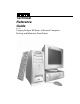
Technical Reference Guide For the Compaq Deskpro EN Series of Personal Computers Desktop and Minitower Form Factors
This hardcopy is designed to be placed into a standard 3-ring binder. Provided below is a title block that can be copied and cut out and placed into the slip or taped onto the edge of the binder.
Reader Feedback Please feel free to send any questions, suggestions, corrections, or comments regarding this document please to the following email address: Desktop.training.feedback@Compaq.com When responding, please state the title of the referenced document.
Technical Reference Guide NOTICE The information in this document is subject to change without notice. COMPAQ COMPUTER CORPORATION SHALL NOT BE LIABLE FOR TECHNICAL OR EDITORIAL ERRORS OR OMISSIONS HEREIN; NOR FOR INCIDENTAL OR CONSEQUENTIAL DAMAGES RESULTING FROM THE FURNISHING, PERFORMANCE, OR USE OF THIS MATERIAL. IT IS THE RESPONSIBILITY OF MANUFACTURERS TO ENSURE THAT DEVICES DESIGNED TO BE USED WITH COMPAQ PRODUCTS COMPLY WITH FCC CLASS B EMISSIONS REQUIREMENTS.
Technical Reference Guide ii Compaq Deskpro EN Series of Personal Computers Desktop and Minitower Form Factors Third Edition–- September1998
Technical Reference Guide TABLE OF CONTENTS CHAPTER 1 INTRODUCTION............................................................................................................. 1.1 ABOUT THIS GUIDE ........................................................................................................... 1-1 1.1.1 USING THIS GUIDE ..................................................................................................... 1-1 1.1.2 ADDITIONAL INFORMATION SOURCES.....................................
Technical Reference Guide CHAPTER 4 SYSTEM SUPPORT......................................................................................................... 4.1 INTRODUCTION.................................................................................................................. 4-1 4.2 PCI BUS OVERVIEW ........................................................................................................... 4-2 4.2.1 PCI CONNECTOR....................................................................
Technical Reference Guide 5.5 PARALLEL INTERFACE ................................................................................................... 5-20 5.5.1 STANDARD PARALLEL PORT MODE ..................................................................... 5-20 5.5.2 ENHANCED PARALLEL PORT MODE ..................................................................... 5-21 5.5.3 EXTENDED CAPABILITIES PORT MODE ............................................................... 5-21 5.5.
Technical Reference Guide 8.3 MEMORY DETECTION AND CONFIGURATION.............................................................. 8-3 8.4 DESKTOP MANAGEMENT SUPPORT ............................................................................... 8-4 8.4.1 SYSTEM ID................................................................................................................... 8-6 8.4.2 SYSTEM INFORMATION TABLE ............................................................................... 8-6 8.4.
Technical Reference Guide APPENDIX C KEYBOARD ................................................................................................................... C.1 INTRODUCTION..................................................................................................................C-1 C.2 KEYSTROKE PROCESSING................................................................................................C-2 C.2.1 TRANSMISSIONS TO THE SYSTEM .........................................................
Technical Reference Guide LIST OF FIGURES FIGURE 2–1. FIGURE 2–2. FIGURE 2–3. FIGURE 2–4. FIGURE 2–5. FIGURE 2–6. FIGURE 2–7. FIGURE 2–8. FIGURE 2–9. COMPAQ DESKPRO EN PERSONAL COMPUTER WITH MONITOR ........................................... 2-1 CABINET LAYOUTS, FRONT VIEW ...................................................................................... 2-4 CABINET LAYOUTS, REAR VIEW ........................................................................................
Technical Reference Guide FIGURE C–1. FIGURE C–2. FIGURE C–3. FIGURE C–4. FIGURE C–5. FIGURE C–6. KEYSTROKE PROCESSING ELEMENTS, BLOCK DIAGRAM ....................................................C-2 KEYBOARD-TO-SYSTEM TRANSMISSION OF CODE 58H, TIMING DIAGRAM ..........................C-3 U.S. ENGLISH (101-KEY) KEYBOARD KEY POSITIONS .......................................................C-4 NATIONAL (102-KEY) KEYBOARD KEY POSITIONS ............................................................C-4 U.S.
Technical Reference Guide LIST OF TABLES TABLE 1–1. ACRONYMS AND ABBREVIATIONS ....................................................................................... 1-3 TABLE 2–1. TABLE 2–2. TABLE 2–3. TABLE 2–4. TABLE 2–5. TABLE 2–6. TABLE 2–7. TABLE 2–8. TABLE 2–9. MODEL DIFFERENCES....................................................................................................... 2-10 SUPPORT CHIPSETS .................................................................................................
Technical Reference Guide TABLE 5–9. TABLE 5–10. TABLE 5–11. TABLE 5–12. TABLE 5–13. TABLE 5–14. TABLE 5–15. TABLE 5–16. TABLE 5–17. TABLE 5–18. TABLE 5–19. TABLE 5–20. TABLE 5–21. DB-9 SERIAL CONNECTOR PINOUT .................................................................................. 5-14 SERIAL INTERFACE CONFIGURATION REGISTERS.............................................................. 5-15 SERIAL INTERFACE CONTROL REGISTERS .....................................................................
Technical Reference Guide TABLE D–1. OPERATING SPECIFICATIONS............................................................................................. D-5 TABLE E–1. TABLE E–2. TABLE E–3. TABLE E–4. TABLE E–5. ULTRA SCSI HOST ADAPTER CARD CONTROL REGISTER MAPPING ......................................E-3 ULTRA SCSI HOST ADAPTER CARD SPECIFICATIONS ...........................................................E-3 WIDE ULTRA SCSI ADAPTER CARD TYPICAL CONFIGURATION ..........................................
Technical Reference Guide Chapter 1 INTRODUCTION 1. Chapter 1 INTRODUCTION 1.1 ABOUT THIS GUIDE This guide provides technical information about the Compaq Deskpro EN Series of Personal Computers in desktop and minitower form factors. This document includes information regarding system design, function, and features that can be used by programmers, engineers, technicians, and system administrators. This and other support documentation is available online and can be downloaded in .
Chapter 1 Introduction 1.2 NOTATIONAL CONVENTIONS 1.2.1 VALUES Hexadecimal values are indicated by the letter “h” following an alpha-numerical value. Binary values are indicated by the letter “b” following a value of ones and zeros. Memory addresses expressed as “SSSS:OOOO” (SSSS = 16-bit segment, OOOO = 16-bit offset) can be assumed as a hexadecimal value. Values that have no succeeding letter can be assumed to be decimal. 1.2.
Technical Reference Guide 1.3 COMMON ACRONYMS AND ABBREVIATIONS Table 1-1 lists the acronyms and abbreviations used in this guide. Table 1–1. Acronyms and Abbreviations Table 1-1.
Chapter 1 Introduction Table 1-1.
Technical Reference Guide Table 1-1.
Chapter 1 Introduction Table 1-1.
Technical Reference Guide Chapter 2 SYSTEM OVERVIEW 2. 2.1 Chapter 2 SYSTEM OVERVIEW INTRODUCTION The Compaq Deskpro EN Series of desktop and minitower Personal Computers (Figure 2-1) delivers an outstanding combination of manageability, serviceability, and consistency for enterprise environments. Based on Intel Pentium II and Celeron processors, the Deskpro EN Series emphasizes performance and industry compatibility. These models feature architectures incorporating the PCI, AGP, and ISA buses.
Chapter 2 System Overview 2.2 FEATURES AND OPTIONS This section describes the standard features and available options. 2.2.1 STANDARD FEATURES The following standard features are included on all models: ♦ ♦ ♦ ♦ ♦ ♦ ♦ ♦ ♦ ♦ ♦ ♦ ♦ ♦ ♦ ♦ ♦ ♦ ♦ 2-2 Pentium II or Celeron processor High-performance 2D/3D AGP graphics card Embedded 16-bit full-duplex audio with Compaq Premier Sound 3.5 inch, 1.
Technical Reference Guide 2.2.2 OPTIONS The following items are available as options for all models and may be included in the standard configuration of some models: ♦ System Memory: 16-MB DIMM (ECC and non-ECC) 32-MB DIMM (ECC and non-ECC) 64-MB DIMM (ECC and nonECC) 128-MB DIMM (ECC and non-ECC) ♦ Hard drives/controllers: 3.2 GB UATA 4.3 GB Wide Ultra SCSI 9.1 GB Wide Ultra SCSI Wide Ultra SCSI PCI controller 6.4 GB UATA ♦ Removeable media drives: 1.
Chapter 2 System Overview 2.3 MECHANICAL DESIGN The Compaq Deskpro EN Series uses a desktop form factor. This section illustrates the mechanical particulars of the bezel, chassis, and major board assemblies. 2.3.1 CABINET LAYOUTS 1 2 3 4 1 2 3 5 5 6 6 7 7 Desktop Item 1 2 3 4 5 6 7 Minitower Function 1.44 MB Diskette Drive (5.25” drive bay) CD-ROM Drive (CDS models) (5.25“ drive bay) Internal Drive (5.25”) bay Internal Drive (3.
Technical Reference Guide 2 1 3 1 2 4 6 9 8 10 12 14 16 20 4 5 6 7 8 11 9 13 3 5 10 15 12 17 14 18 16 19 20 7 11 13 15 17 18 19 Desktop Item 1 2 3 4 5 6 7 8 9 10 11 12 13 14 15 16 17 18 19 20 Minitower Function AC Line In Connector Smart Cover Lock Screws Line Voltage Switch USB Interface Port B USB Interface Port A 100TX speed LED Activity LED Link LED NIC Connector SCSI connector Audio Headphone Input Audio Microphone Input Audio Line Output Audio Line Input Keyboard Connec
Chapter 2 System Overview 2.3.2 CHASSIS LAYOUTS Figures 2-4 and 2-5 show the layout of key assemblies within the desktop and minitower chassis respectively. For serviceability this system features an expansion card cage that allows easy removal of the backplane and expansion cards as a single assembly. The tilt drive cage tilts up for easy removal/replacement of drives.
Technical Reference Guide ISA Slot Power Supply ISA Slot PCI Slot 5 PCI Slot 4 Drive Bays PCI Slot 3 PCI Slot 2 (SCSI Card) Expansion Card Cage PCI Slot 1 (NIC Card) Slots On Backplane, Rear View @ 90° Front Back Wide-Ultra SCSI Card Processor System Board Speaker AGP NLX Graphics Card Figure 2–5.
Chapter 2 System Overview 2.3.3 BOARD LAYOUTS Figure 2-6 shows the location of connectors and switches for the system board, which is the same for all models and both formfactors.
Technical Reference Guide Figure 2-7 shows the connector and switch locations for the two types of backplane boards.
Chapter 2 System Overview 2.4 SYSTEM ARCHITECTURE The Compaq Deskpro EN Series of Personal Computers is based on an Intel Pentium II processor matched with the Intel 440BX AGPset. The basic architecture (Figure 2-8), uses three main buses: the Host bus, the Peripheral Component Interconnect (PCI) bus, and the Industry Standard Architecture (ISA) bus.
Technical Reference Guide Pentium II or Celeron Processor 66-/100- MHz 64-Bit Host Bus 66-MHz 32-Bit AGP Bus Graphics Cntlr. Card 82443BX (North Bridge) 66-/100-MHz 64-Bit Mem. Bus 33-MHz 32-Bit PCI Bus Pri. IDE I/F Sec. IDE I/F Wide Ultra SCSI Hard Drive Wide Ultra SCSI Cntlr.
Chapter 2 System Overview 2.4.1 PROCESSOR The Deskpro EN Series includes models based on Pentium II and Celeron processors. The processor and heat sink is mounted as an assembly (Figure 2-9) in a slot (Slot 1) on the system board. The Pentium II processor includes a microprocessor and a secondary (L2) cache contained in a single edge connector (SEC) cartridge to which a heat sink is attached. The Celeron processor includes a microprocessor mounted on a single edge processor package (SEPP) board.
Technical Reference Guide 2.4.2 SYSTEM MEMORY This system provides three 168-pin DIMM sockets with 16, 32 or 64 megabytes of RAM installed depending on model. System memory can be expanded up to 384 megabytes using 16-, 32-, 64-, and 128-MB DIMMs. This system supports SDRAM, EDO, and ECC DIMMs. Models 3200 and 6400 come with SDRAM installed while models 4300 and 9100 come with ECC DIMMs installed. Non-parity DIMMs are installed as standard but parity DIMMs are supported. 2.4.
Chapter 2 System Overview 2.4.5 SERIAL AND PARALLEL INTERFACES All models include two serial ports and a parallel port accessible at the rear of the chassis. The serial and parallel ports are integrated into a PC87307 I/O Controller component. The serial port is RS-232-C/16550-compatible and operates at baud rates up to 115,200. The parallel interface is Enhanced Parallel Port (EPP1.9) and Enhanced Capability Port (ECP) compatible, and supports bi-directional data transfers. 2.4.
Technical Reference Guide 2.5 SPECIFICATIONS This section includes the environmental, electrical, and physical specifications for the Compaq DESKPRO EN Series Personal Computers. Table 2–4. Environmental Specifications Table 2-4. Environmental Specifications Parameter Operating o o o o Air Temperature 50 to 95 F (10 to 35 C) Shock N/A Vibration 0.000215g^ 2/hz, 10-300 Hz [1] o Humidity 90% RH @ 36 C (no hard drive) Maximum Altitude 10,000 ft (3048 m) NOTE: Values are subject to change without notice.
Chapter 2 System Overview Table 2–7. Diskette Drive Specifications Table 2-7. Diskette Drive Specifications (Compaq SP# 179161-001) Parameter Media Type Height Bytes per Sector Sectors per Track: High Density Low Density Tracks per Side: High Density Low Density Read/Write Heads Average Access Time: Track-to-Track (high/low) Average (high/low) Settling Time Latency Average Measurement 3.5 in 1.44 MB/720 KB diskette 1/3 bay (1 in) 512 18 9 80 80 2 3 ms/6 ms 94 ms/173ms 15 ms 100 ms Table 2–8.
Technical Reference Guide Table 2–9. Hard Drive Specifications Table 2-9. Hard Drive Specifications Parameter Interface Drive Type Drive Size Transfer Rate Seek Time (w/settling) Single Track Average Full Stroke Disk Format: # of Cylinders # of Data Heads # of Sectors per Track Buffer Size Drive Fault Prediction 3.2 GB (# 166873-001) EIDE-UATA 65 5.25 in 33.3 MB/s 4.3 GB (# 179287-001) Wide-Ultra SCSI 65 5.25 in 40.0 MB/s 6.4 GB (# 166973-001) EIDE-UATA 65 5.25 in 33.3 MB/s 9.
Chapter 2 System Overview This page is intentionally blank.
Technical Reference Guide Chapter 3 PROCESSOR/ MEMORY SUBSYSTEM 3. Chapter 3 PROCESSOR/MEMORY SUBSYSTEM 3.1 INTRODUCTION This chapter describes the processor/cache memory subsystem of the Compaq Deskpro EN Series of desktop and minitower Personal Computers. These systems are shipped either with an Intel Pentium II or Celeron processor and either 32 or 64 megabytes of system memory, depending on configuration. This chapter includes the following topics: ♦ Processor/memory subsystem [3.
Chapter 3 Processor/Memory Subsystem 3.2 PROCESSOR/MEMORY SUBSYSTEM The subsystem features an Intel Pentium II or Celeron processor with the North Bridge (82443BX), and either 32 or 64 megabytes of system memory (Figure 3-1). The 64-bit Host and memory buses operate at either 66- or 100-MHz depending on the speed of the processor. The 32bit PCI bus operates at 33-MHz.
Technical Reference Guide 3.2.1 PROCESSOR The system board includes a Slot 1-type interface that accommodates a Pentium II or Celeron processor. Table 3-1 provides a comparison between the key parameters of the Pentium II and Celeron processors. Table 3–1. Processor Comparison Table 3-1. Processor Comparsion CPU Freq. L2 Cache L2 Cache Freq. Host Bus Freq.
Chapter 3 Processor/Memory Subsystem 3.2.1.2 Celeron Processor Select systems are shipped with the Intel Celeron processor. The Celeron processor (Figure 3-3) uses a CPU/FPU core that is functionally the same as that of the Pentium II described previously and provides the same level of branch prediction, math co-processing, MMX support, and L1 cache operation. Processing and Host bus speed ratios follow those of the Pentium II processors and are set and determined with the same methods.
Technical Reference Guide 3.2.2 PROCESSOR CHANGING/UPGRADING The slot 1 design allows for easy changing and/or upgrading of the processor/cache complex. Changing the processor requires disconnection/re-connection of the heat sink sensor cable and may require upgrading the BIOS firmware and re-configuration of the bus/core speed switch discussed in the following paragraphs. 3.2.2.1 BIOS Upgrading The Pentium II 450 and Celeron 300A/333 processors require BIOS firmware dated 7/30/98 or later.
Chapter 3 Processor/Memory Subsystem 3.2.3 SYSTEM MEMORY The system board contains three 168-pin DIMM sockets for system memory. This system is designed for using SDRAM or ECC DIMMs. As shipped from the factory the standard configuration has 16, 32, or 64 megabytes of memory installed. The system memory is expandable up to a maximum of 384 megabytes. Single or double-sided DIMMs may be used.
Technical Reference Guide Table 3–3. SPD Address Map (SDRAM DIMM) Table 3-3. SPD Address Map (SDRAM DIMM) Byte 0 1 2 3 4 5 6, 7 8 9 10 11 12 13 14 15 16 17 18 19 20 21 22 23 24 25 26 NOTES: Description No. of Bytes Written Into EEPROM Total Bytes (#) In EEPROM Memory Type No. of Row Addresses On DIMM No. of Column Addresses On DIMM No. of Module Banks On DIMM Data Width of Module Voltage Interface Standard of DIMM Cycletime @ Max CAS Latency (CL) Access From Clock Config. Type (Parity, Nonparity, etc.
Chapter 3 Processor/Memory Subsystem Figure 3-3 shows the system memory map for the system. FFFF FFFFh FFE0 0000h FFDF FFFFh FEC1 0000h FEC0 FFFFh FEC0 0000h FEBF FFFFh 4 GB High BIOS Area (2 MB) PCI Memory (18 MB) APIC Config.
Technical Reference Guide 3.2.4 SUBSYSTEM CONFIGURATION The 443BX north bridge component provides the configuration function for the processor/memory subsystem. Table 3-4 lists the configuration registers used for setting and checking such parameters as memory control and PCI bus operation. These registers reside in the PCI Configuration Space and accessed using the methods described in Chapter 4, section 4.2. Table 3–4. Host/PCI Bridge Configuration Registers (443BX, Function 0) Table 3-4.
Chapter 3 Processor/Memory Subsystem This page is intentionally blank.
Technical Reference Guide Chapter 4 SYSTEM SUPPORT 4. Chapter 4 SYSTEM SUPPORT 4.1 INTRODUCTION This chapter covers subjects dealing with basic system architecture and covers the following topics: ♦ ♦ ♦ ♦ ♦ ♦ ♦ PCI bus overview (4.2) page 4-2 AGP bus overview (4.3) page 4-11 ISA bus overview (4.4) page 4-16 System clock distribution (4.5) page 4-28 Real-time clock and configuration memory (4.6) page 4-29 I/O map and register accessing (4.7) page 4-46 System management (4.
Chapter 4 System Support 4.2 PCI BUS OVERVIEW NOTE: This section describes the PCI bus in general and highlights bus implementation in this particular system. For detailed information regarding PCI bus operation, refer to the PCI Local Bus Specification Revision 2.1. This system implements a 5-V, 32-bit Peripheral Component Interconnect (PCI) bus operating at 33 MHz. The PCI bus uses a shared address/data bus design. On the first clock cycle of a PCI bus transaction the bus carries address information.
Technical Reference Guide 4.2.1 PCI CONNECTOR B94 B62 A62 A94 B1 B49 B52 A52 A1 A49 Figure 4–2. PCI Bus Connector (32-Bit Type) Table 4–1. PCI Bus Connector Pinout Table 4-1. PCI Bus Connector Pinout Pin 01 02 03 04 05 06 07 08 09 10 11 12 13 14 15 16 17 18 19 20 21 22 23 24 25 26 27 28 29 30 31 -- B Signal -12 VDC TCK GND TDO +5 VDC +5 VDC INTBINTDPRSNT1RSVD PRSNT2GND GND RSVD GND CLK GND REQ+5 VDC AD31 AD29 GND AD27 AD25 +3.3 VDC C/BE3AD23 GND AD21 AD19 +3.
Chapter 4 System Support 4.2.2 PCI BUS MASTER ARBITRATION The PCI bus supports a bus master/target arbitration scheme. A bus master is a device that has been granted control of the bus for the purpose of initiating a transaction. A target is a device that is the recipient of a transaction. Request (REQ), Grant (GNT), and FRAME signals are used by PCI bus masters for gaining access to the PCI bus.
Technical Reference Guide 4.2.3 PCI BUS TRANSACTIONS The PCI bus consists of a 32-bit path (AD31-00 lines) that uses a multiplexed scheme for handling both address and data transfers. A bus transaction consists of an address cycle and one or more data cycles, with each cycle requiring a clock (PCICLK) cycle.
Chapter 4 System Support Figure 4-3 shows how the loading of 0CF8h results in a Type 0 configuration cycle on the PCI bus. The Device Number (bits <15..11> determines which one of the AD31..11 lines is to be asserted high for the IDSEL signal, which acts as a “chip select” function for the PCI device to be configured. 31 30 24 23 Reserved Register 0CF8h 16 15 11 10 8 7 2 1 0 Bus Device Function Register 0 0 Number Number Number Index Results in: 31 AD31..0 w/Type 0 Config.
Technical Reference Guide Table 4–4. PCI Function Configuration Acces Table 4-4. PCI Function Configuration Access PCI Function Host/PCI Bridge (82443) PCI/AGP Bridge (82443) PCI/ISA Bridge (82371) IDE Interface (82371) USB Interface (82371) Power Management Cntlr. (82371) Device No. 0 0 20 20 20 20 Function No. 0 1 0 1 2 3 The register index (CF8h, bits <7..2>) identifies the 32-bit location within the configuration space of the PCI device to be accessed.
Chapter 4 System Support Table 4–5. System Board PCI Device Identification Table 4-5. System Board PCI Device Identification PCI Device Vender ID Device ID North Bridge (82443 PAC): Host/PCI Bridge (Function 0) 8086h 7190h PCI/AGP Bridge (Function 1) [1] 8086h 7191h South Bridge (82371 PIIX4): 7110h 8086h PCI/ISA Bridge (Function 0) 7111h 8086h EIDE Controller (Function 1) 7112h 8086h USB I/F (Function 2) 7113h 8086h Power Mngmt.
Technical Reference Guide 4.2.5 PCI INTERRUPT MAPPING The PCI bus provides for four interrupt signals; INTA-, INTB-, INTC-, and INTD-. These signals may be generated by on-board PCI devices or by devices installed in the PCI slots. In order to minimize latency, INTA-..INTD- signal routing from the interrupt controller of the 82371south bridge to PCI slots/devices is distributed evenly as shown below: Interrupt Cntlr.
Chapter 4 System Support 4.2.7 PCI CONFIGURATION PCI bus operations, especially those that involve ISA bus interaction, require the configuration of certain parameters such as PCI IRQ routing, top of memory accessible by ISA, SMI generation, and clock throttling characteristics. These parameters are handled by the PCI/ISA bridge function (PCI function #0) of the South Bridge component and configured through the PCI configuration space registers listed in Table 4-6.
Technical Reference Guide 4.3 AGP BUS OVERVIEW NOTE: This section describes the AGP bus in general. For a detailed description of AGP bus operations refer to the AGP Interface Specification available at the following AGP forum web site: http://www.agpforum.org/index.htm The Accelerated Graphics Port (AGP) bus is specifically designed as an economical yet highperformance interface for 3D graphics adapters.
Chapter 4 System Support 4.3.1.1 Data Request Requesting data is accomplished in one of two ways; either multiplexed addressing (using the AD lines for addressing/data) or demultiplexed (“sideband”) addressing (using the SBA lines for addressing only and the AD lines for data only). Even though there are only eight SBA lines (as opposed to the 32 AD lines) sideband addressing maximizes efficiency and throughput by allowing the AD lines to be exclusively used for data transfers.
Technical Reference Guide AGP 2X Transfers In AGP 2X transfers, clocking is basically the same as in 1X transfers except that the 66-MHz CLK signal is used to qualify only the control signals. The data bytes are latched by an additional strobe (AD_STBx) signal so that an 8-byte transfer occurs in one CLK cycle (Figure 4-6). The first four bytes (DnA) are latched by the receiving agent on the falling edge of AD_STBx and the second four bytes (DnB) are latched on the rising edge of AD_STBx.
Chapter 4 System Support 4.3.2 AGP CONFIGURATION AGP bus operations require the configuration of certain parameters involving system memory access by the AGP graphics adapter. The AGP bus interface is configured as a PCI device integrated within the north bridge (82443, device 1) component. The AGP function is, from the PCI bus perspective, treated essentially as a PCI/PCI bridge and configured through PCI configuration registers (Table 4-7). Configuration is accomplished by BIOS during POST.
Technical Reference Guide 4.3.3 AGP CONNECTOR B94 A1 A21 B1 A94 A66 A26 B21 B66 B26 Figure 4–7. AGP Bus Connector Table 4–8. AGP Bus Connector Pinout Table 4-8.
Chapter 4 System Support 4.4 ISA BUS OVERVIEW NOTE: This section describes the ISA bus in general and highlights bus implementation in this particular system. For detailed information regarding ISA bus operation, refer to the Compaq Extended Industry Standard Architecture (EISA) Technical Reference Guide. The industry standard architecture (ISA) bus provides an 8-/16-bit path for standard I/O peripherals as well as for optional devices that can be installed in the ISA expansion slots.
Technical Reference Guide 4.4.1 ISA CONNECTOR 16-Bit ISA Connection 8-Bit ISA Connection D1 B1 C1 A1 Figure 4–9. ISA Expansion Connector Table 4–9. ISA Expansion Connector Pinout Table 4-9.
Chapter 4 System Support 4.4.2 ISA BUS TRANSACTIONS The ISA bus supports 8- and 16-bit transfers at an 8-MHz rate. Devices limited to 8-bit transfers use the lower byte portion (data lines 7..0) while 16-bit transfers use the full bandwidth (data lines 15..0). Addressing is handled by two classifications of address signals: latched and latchable. Latched address signals ( SA19..0) select the specific byte within the 1-MB section of memory defined by address lines LA23..17. Latchable address lines (LA23..
Technical Reference Guide When the address changes, devices on the bus may decode the latchable address (LA23..17) lines and then latch them. This arrangement allows devices to decode chip selects and M16- before the next cycle actually begins. The following guidelines apply to optional ISA devices installed in the system: ♦ ♦ ♦ ♦ On bus lines that can be driven by a controller board, the driver should be able to sink a minimum of 20 ma at 0.5 VDC and source 2 ma at 3.75 VDC.
Chapter 4 System Support 4.4.3 DIRECT MEMORY ACCESS Direct Memory Access (DMA) is a method by which an ISA device accesses system memory without involving the microprocessor. DMA is normally used to transfer blocks of data to or from an ISA I/O device. DMA reduces the amount of CPU interactions with memory, freeing the CPU for other processing tasks. NOTE: This section describes DMA in general.
Technical Reference Guide 4.4.3.1 Page Registers The DMA page register contains the eight most significant bits of the 24-bit address and works in conjunction with the DMA controllers to define the complete (24-bit)address for the DMA channels. Table 4-11 lists the page register port addresses. Table 4–11. DMA Page Register Addresses Table 4-11.
Chapter 4 System Support The RAM refresh is designed to perform a memory read cycle on each of the 512 row addresses in the DRAM memory space. Refresh operations are used to refresh memory on the 32-bit memory bus and the ISA bus. The refresh address is provided on lines SA00 through SA08. Address lines LA23..17, SA18,19 are driven low. The remaining address lines are in an undefined state during the refresh cycle. The refresh operations are driven by a 69.
Technical Reference Guide 4.4.4 INTERRUPTS The microprocessor uses two types of interrupts; maskable and nonmaskable. A maskable interrupt can be enabled or disabled within the microprocessor by the use of the STI and CLI instructions. A nonmaskable interrupt cannot be masked off within the microprocessor but may be inhibited by hardware or software means external to the microprocessor. 4.4.4.
Chapter 4 System Support Table 4–13. Maskable Interrupt Priorities and Assignments Table 4-13.
Technical Reference Guide 4.4.4.2 Non-Maskable Interrupts Non-maskable interrupts cannot be masked (inhibited) within the microprocessor itself but may be maskable by software using logic external to the microprocessor. There are two non-maskable interrupt signals: the NMI- and the SMI-. These signals have service priority over all maskable interrupts, with the SMI- having top priority over all interrupts including the NMI-.
Chapter 4 System Support SMI- Generation The SMI- (System Management Interrupt) is typically used for power management functions. When power management is enabled, inactivity timers are monitored. When a timer times out, SMI- is asserted and invokes the microprocessor’s SMI handler. The SMI- handler works with the APM BIOS to service the SMI- according to the cause of the timeout.
Technical Reference Guide 4.4.5 INTERVAL TIMER The interval timer generates pulses at software (programmable) intervals. A 8254-compatible timer is integrated into the South Bridge chip. The timer function provides three counters, the functions of which are listed in Table 4-15. Table 4–15. Interval Timer Functions Table 4-15. Interval Timer Functions Counter 0 1 2 Function System Clock Refresh Speaker Tone Gate Always on Always on Port 61, bit<0> Clock In 1.193 MHz 1.193 MHz 1.
Chapter 4 System Support 4.5 SYSTEM CLOCK DISTRIBUTION The system uses a Cypress CY2280 or compatible part for generation of most clock signals. Table 4-17 lists the system board clock signals and how they are distributed. Table 4–17. Clock Generation and Distribution Table 4-17. Clock Generation and Distribution Frequncy/Signal Source Destination 66, 100 MHz CY2280 Processor, 82443 N. Bridge (CPUCLK) [1] 66 MHz North Bridge AGP Slot 48 MHz “ 82371 S. Bridge, 87307 I/O Cntlr.
Technical Reference Guide 4.6 REAL-TIME CLOCK AND CONFIGURATION MEMORY The Real-time clock (RTC) and configuration memory functions are provided by the PC87307 I/O controller. The RTC uses the first 14 of 256 bytes of configuration memory and is MC146818-compatible. As shown in the following figure, the 87307 controller provides 256 bytes of configuration memory, divided into two 128-byte banks.
Chapter 4 System Support Table 4-18 lists the mapping of the configuration memory. Locations 00h-3Fh may be accessed using OUT/IN assembly language instructions or BIOS function INT15, AX=E823h. All other locations should be accessed using the INT15, AX=E845h function (refer to Chapter 8 for BIOS function descriptions). Table 4–18. Configuration Memory (CMOS) Map Table 4-18.
Technical Reference Guide RTC Control Register A, Byte 0Ah Bit 7 6..4 3..0 Function Update in Progress. Read only. 0 = Time update will not occur before 2444 us 1 = Time update will occur within 2444 us Divider Chain Control. R/W. 00x = Oscillator disabled. 010 = Normal operation (time base frequency = 32.768 KHz). 11x = Divider chain reset. Periodic Interrupt Control. R/W. Specifies the periodic interrupt interval. 0000 = none 1000 = 3.90625 ms 0001 = 3.90625 ms 1001 = 7.8125 ms 0010 = 7.
Chapter 4 System Support 6..0 Reserved Configuration Byte 0Eh, Diagnostic Status Default Value = 00h This byte contains diagnostic status data. Configuration Byte 0Fh, System Reset Code Default Value = 00h This byte contains the system reset code. Configuration Byte 10h, Diskette Drive Type Bit Function 7..4 Primary (Drive A) Diskette Drive Type 3..0 Secondary (Drive B) Diskette Drive Type Valid values for bits <7..4> and bits <3..0>: 0000 = Not installed 0001 = 360-KB drive 0010 = 1.
Technical Reference Guide Configuration Byte 13h, Security Functions Default Value = 00h Bit Function 7 Reserved 6 QuickBlank Enable After Standby: 0 = Disable 1 = Enable 5 Administrator Password: 0 = Not present 1 = Present 4 Reserved 3 Diskette Boot Enable: 0 = Enable 1 = Disable 2 QuickLock Enable: 0 = Disable 1 = Enable 1 Network Server Mode/Security Lock Override: 0 = Disable 1 = Enable 0 Password State (Set by BIOS at Power-up) 0 = Not set 1 = Set Configuration Byte 14h, Equipment Installed Default
Chapter 4 System Support Configuration Bytes 19h-1Ch, Hard Drive Types Byte 19h contains the hard drive type for drive 1 of the primary controller if byte 12h bits <7..4> hold 1111b. Byte 1Ah contains the hard drive type for drive 2 of the primary controller if byte 12h bits <3..0> hold 1111b. Bytes1Bh and 1Ch contain the hard drive types for hard drives 1 and 2 of the secondary controller.
Technical Reference Guide Configuration Byte 26h, Auxiliary Peripheral Configuration Default Value = 00h Bit Function 7,6 I/O Delay Select 00 = 420 ns (default) 01 = 300 ns 10 = 2600 ns 11 = 540 ns 5 Alternative A20 Switching 0 = Disable port 92 mode 1 = Enable port 92 mode 4 Bi-directional Print Port Mode 0 = Disabled 1 = Enabled 3 Graphics Type 0 = Color 1 = Monochrome 2 Hard Drive Primary/Secondary Address Select: 0 = Primary 1 = Secondary 1 Diskette I/O Port 0 = Primary 1 = Secondary 0 Diskette I/O Por
Chapter 4 System Support Configuration Byte 29h, Miscellaneous Configuration Data Default Value = 00h Bit Function 7..5 Reserved 4 Primary Hard Drive Enable (Non-PCI IDE Controllers) 0 = Disable 1 = Enable 3..0 Reserved Configuration Byte 2Ah, Hard Drive Timeout Default Value = 02h Bit Function 7..5 Reserved 4..0 Hard Drive Timeout 00000 = Disabled 00001 = 1 minute 00010 = 2 minutes . .
Technical Reference Guide Configuration Byte 2Dh, Additional Flags Default Value = 00h Bit Function 7..5 Reserved 4 Memory Test 0 = Test memory on power up only 1 = Test memory on warm boot 3 POST Error Handling (BIOS Defined) 0 = Display “Press F1 to Continue” on error 1 = Skip F1 message 2..0 Reserved Configuration Byte 2Eh, 2Fh, Checksum These bytes hold the checksum of bytes 10h to 2Dh.
Chapter 4 System Support Configuration Byte 35h, APM Status Flags Default Value = 11h Bit Function 7..
Technical Reference Guide Configuration Byte 45h, Keyboard Snoop Data Default Value = xxh Bit Function 7 Cntrl/F10 Key Status: 0 = Cntrl & F10 keys not pressed 1 = Cntrl & F10 keys pressed 6 F10 Key Status: 0 = F10 key not pressed 1 = F10 key pressed 5..
Chapter 4 System Support Configuration Byte 52h, Board Revision This byte holds the board revision as copied from the boot block sector. Configuration Byte 53h, 54h, SW SMI Command/Data Bytes Configuration Byte 55h, APM Command Byte Configuration Byte 56h, Miscellaneous Flags Byte Bit 7 6 5 4 3..1 0 Function CAS Latency: 0 = 2, 1 = 3 IR Port Enable Flag: 0 = Disabled (COM2 config. for standard serial port) 1 = Enabled (COM2 config.
Technical Reference Guide Configuration Byte 83h, Microprocessor Identification This byte holds the component ID and chip revision of the microprocessor. Configuration Byte 84h, Microprocessor Revision Configuration Byte 85h, Administration Mode Bit 7,6 5 4 3 2 1 0 Function Reserved ESCD Buffering: 0 = No buffering, 1 = ESCD buffered at F000h.
Chapter 4 System Support Configuration Byte 90h, 91h, Total Super Extended Memory Configured This byte holds the value of the amount of extended system memory that is configured. The amount is given in 64-KB increments. Configuration Byte 92h, Miscellaneous Configuration Byte Default Value = 18h Bit Function 7..5 Reserved 4 Diskette Write Control: 0 = Disable 1 = Enable 3..
Technical Reference Guide Configuration Byte 94h, ROM Flash/Power Button Status Default Value = 00h Bit Function 7..5 Reserved 4 ROM Flash In Progress (if set) 3 Reserved 2 Power Button Inhibited (if set) 1 User-Forced Bootblock (if set) 0 ROM Flash In Progress (if set) Configuration Byte 97h, Asset/Test Prompt Byte Default Value = 00h Bit Function 7,6 Test Prompt: 01 = Fake F1 10 = Fake F2 11 = Fake F10 5..0 Asset Value Configuration Byte 9Bh, Ultra-33 DMA Enable Byte Default Value = 00h Bit Function 7.
Chapter 4 System Support Configuration Byte 9Dh, ESS Audio Configuration Byte Default Value = 12h Bit Function 7 Reserved for Game Port Enable 6,5 Audio Address 00 = 22xh 01 = 23xh 10 = 24xh 11 = 25xh 4,3 DMA Channel 00 = Disabled 01 = DMA0 10 = DMA1 11 = DMA3 2,1 IRQ Select 00 = IRQ9 01 = IRQ5 10 = IRQ7 11 = IRQ10 0 ESS Audio Chip Enable 0 = Enabled 1 = Disabled Configuration Byte 9Eh, ECP DMA Configuration Byte Default Value = 03h Bit Function 7..4 Reserved 3 SafeStart Control: 0 = Disable 1 = Enable 2.
Technical Reference Guide Configuration Byte C7h, C8h, Serial Ports 1 and 2 (Respectively) Configuration Bytes Default Value = FEh, 7Dh Bit Function 7..2 Base I/O Address (in packed format) (Algorithm: [Addr. - 200h] / 8) (i.e., 3Fh = 3F8h, 1Fh = 2F8h, 00 = 200h) 1..
Chapter 4 System Support 4.7 I/O MAP AND REGISTER ACCESSING 4.7.1 SYSTEM I/O MAP Table 4–19. System I/O Map Table 4-19. System I/O Map I/O Port Function 0000..000Fh DMA Controller 1 0020..0021h Interrupt Controller 1 0040..
Technical Reference Guide 4.7.2 GPIO UTILIZATION This section describes the utilization of general purpose input/output (GPIO) ports provided by the south bridge (82371) and I/O controller (87307) components used in this system. 4.7.2.1 82371 South Bridge GPIO Utilization The 82371 South Bridge component includes a number of single and dual purpose pins available as general purpose input/output (GPIO) ports.
Chapter 4 System Support Table 4–21. 82371 South Bridge General Purpose Output Port Utilization Table 4-21. 82371 South Bridge General Purpose Output Port Utilization GP Output Port GPO #0 GPO #1-7 GPO #8 GPO #9 GPO #10 GPO #11 GPO #12 GPO #13 GPO #14 GPO #15 GPO #16 GPO #17 GPO #18 GPO #19 GPO #20 GPO #21 GPO #22, 23 GPO #24 GPO #25 GPO #26 GPO #27 GPO #28-30 Function PCI reset. When low will generate a PCI RST- to PCI slots. ISA bus address signals LA17-23. Not used. Not used. Not used. Not used.
Technical Reference Guide 4.7.2.2 87307 I/O Controller Functions The 87307 I/O controller contains various functions such as the keyboard/mouse interfaces, diskette interface, serial interfaces, and parallel interface. While the control of these interfaces uses standard AT-type I/O addressing, the configuration of these functions uses indexed ports unique to the 87307.
Chapter 4 System Support 87307 GPIO Utilization The 87307 I/O Controller provides 11 general purpose pins that can be individually configured as either inputs or outputs. These pins are mapped as two general purpose ports and utilized as shown below. GPIO Port 1 Data, I/O Addr. 078h, (87307 I/O Controller), Bit 7 6 5 4 3..0 Function GPIO17 (not used) GPIO16 (config. as input): Cover Lock Detect. Read 0, no solenoid Read 1, solenoid GPIO15 (config. as output): Cover Alarm Clear. Write 0 to clear alarm.
Technical Reference Guide 4.8 SYSTEM MANAGEMENT SUPPORT This section describes the hardware support of functions involving security, safety, identification, and power consumption of the system. System management functions are handled largely by a System Security ASIC. Most functions are controlled through registers (Table 4-23) accessed using the indexed method through I/O ports 0C50h (index) and 0C51h (Data). Table 4–23. System Management Control Registers Table 4-23.
Chapter 4 System Support 4.8.1 FLASH ROM WRITE PROTECT The system BIOS firmware is contained in a flash ROM device that can be re-written with updated code if necessary. The ROM is write-protected with a Black Box* security feature. The Black Box feature uses the Administrator password to protect against unauthorized writes to the flash ROM. During the boot sequence, the BIOS checks for the presence of the ROMPAQ diskette.
Technical Reference Guide 4.8.3 I/O SECURITY The 87307 I/O controller allows various I/O functions to be disabled through configuration registers.
Chapter 4 System Support 4.8.5 TEMPERATURE SENSING This system employs two sensors for monitoring the temperature inside the chassis. A thermister attached to the heat sink of the Pentium II SEC cartridge is used to detect the caution level. This thermister, connected to the system board through header P15, is part of sensing logic that provides input to a Compaq ASIC. The sensing logic is set to trip when 179.6 °F (82 °C) is reached.
Technical Reference Guide 4.8.6 SMART COVER LOCK The chassis cover (also known as the “hood”) can be locked to prevent unauthorized personnel from removing the cover and changing the system hardware. The locking mechanism consists of a solenoid controlled by the Setup utility through the Client Management logic in a Compaq ASIC. The presence of the Smart Cover Lock (actually of the solenoid) is detected by logic and readable by software at 87307 GPIO port 1 bit <6>.
Chapter 4 System Support 4.8.8 POWER MANAGEMENT This system provides baseline hardware support of ACPI- and APM-compliant firmware and software. The major power-consuming components (processor, chipset, I/O controller, and fan) can be placed into a reduced power mode upon software command either automatically or by user control. The system can then be brought back up (“wake-up”) by events defined by the ACPI specification.
Technical Reference Guide 4.8.8.3 Hard Drive Spindown Control The timeout parameter stored in the SIT record 04h and indexed through CMOS location 2Ah (bits <4..0>) represents the period of hard drive inactivity required to elapse before the hard drive is allowed to spin down. The timeout value is downloaded from CMOS to a timer on the hard drive. The timeout period can be set in incremental values of 0 (timeout disabled), 10, 15 (default), 20, 30, and 60 minutes.
Chapter 4 System Support This page is intentionally blank.
Technical Reference Guide Chapter 5 INPUT/OUTPUT INTERFACES 5. 5.1 Chapter 5 INPUT/OUTPUT INTERFACES INTRODUCTION This chapter describes the standard (i.e., system board) interfaces that provide input and output (I/O) porting of data and specifically discusses interfaces that are controlled through I/O-mapped registers. The I/O interfaces are integrated functions of the south bridge (82371) and the I/O controller (87307). The following I/O interfaces are covered in this chapter: ♦ ♦ ♦ ♦ ♦ ♦ 5.
Chapter 5 Input/Output Interfaces 5.2.1.1 IDE Configuration Registers The IDE controller is integrated into the south bridge (82371) component and configured as a PCI device with bus mastering capability. The PCI configuration registers for the IDE controller function (PCI device #20, function #1) are listed in Table 5-1. Table 5–1. IDE PCI Configuration Registers Table 5-1. EIDE PCI Configuration Registers (82371 Function 1) PCI Conf. Addr.
Technical Reference Guide 5.2.1.3 IDE ATA Control Registers The IDE controller of the 82586 decodes the addressing of the standard AT attachment (ATA) registers for the connected drive, which is where the ATA control registers actually reside. The primary and secondary interface connectors are mapped as shown in Table 5-3. Table 5–3. IDE ATA Control Registers Table 5-3. IDE ATA Control Registers Primary I/O Addr. 1F0h 1F1h 1F1h 1F2h 1F3h 1F4h 1F5h 1F6h 1F7h 1F7h 3F6h 3F6h 3F7h 3F7h Secondary I/O Addr.
Chapter 5 Input/Output Interfaces The contents of the Error register are interpreted as a diagnostic status byte after the execution of a diagnostic command or when the system is initialized.
Technical Reference Guide Drive Select/Head Register, I/O Port 1F6h/176h Bit 7 6,5 4 3..
Chapter 5 Input/Output Interfaces Command Register, I/O Port 1F7h/177h (Write Only) The IDE controller commands are written to this register. The command write action should be prefaced with the loading of data into the appropriate registers. Execution begins when the command is written to 1F7h/177h. Table 5-4 lists the standard IDE commands. Table 5–4. IDE Controller Commands Table 5-4.
Technical Reference Guide Drive Control Register, I/O Port 3F6h/376h (Write Only) Bit 7..3 2 1 0 Function Reserved Controller Control: 0 = Re-enable 1 = Reset Interrupt Enable/Disable 0 = Disable interrupts 1 = Enable interrupts Reserved Drive Access Register, I/O Port 3F7h/377h (Read Only) Bit 7 6 5..
Chapter 5 Input/Output Interfaces 5.2.2 IDE CONNECTOR This system uses a standard 40-pin connector for IDE devices. Device power is supplied through a separate connector. Figure 5–1. 40-Pin IDE Connector. Table 5–5. 40-Pin IDE Connector Pinout Table 5-5.
Technical Reference Guide 5.3 DISKETTE DRIVE INTERFACE The diskette drive interface supports up to two diskette drives, each of which connect to a standard 34-pin diskette drive connector. All models come standard with a 3.5-inch 1.44-MB diskette drive installed as drive A. An additional diskette drive (either a 3.5-inch 720-KB, 1.44MB, or 2.88-MB drive or a 5.25-inch 360-KB or 1.2-MB drive) may also be installed as drive B.
Chapter 5 Input/Output Interfaces 5.3.1 DISKETTE DRIVE PROGRAMMING 5.3.1.1 Diskette Drive Interface Configuration The diskette drive controller must be configured for a specific address and also must be enabled before it can be used. Address selection and enabling of the diskette drive interface are affected by firmware through the PnP configuration registers of the 87307 I/O controller. The PnP configuration registers are accessed through I/O registers 15Ch (index) and 15Dh (data).
Technical Reference Guide 5.3.1.2 Diskette Drive Interface Control The BIOS function INT 13 provides basic control of the diskette drive interface. The diskette drive interface can be controlled by software through I/O-mapped registers listed in Table 5-7. Table 5–7. Diskette Drive Controller Registers Table 5-7.
Chapter 5 Input/Output Interfaces Main Status Register, I/O Port 3F4h/374h (Read Only) Bit 7 6 5 4 3..0 Function Request for Master. When set, indicates the controller is ready to send or receive data from the CPU. Cleared immediately after a byte transfer. Indicates interrupt pin status during nonDMA phase. Data I/O Direction. 0 = Expecting a write 1 = Expecting a read Non-DMA Execution. When set, indicates controller is in the execution phase of a byte transfer in non-DMA mode. Command In Progress.
Technical Reference Guide 5.3.2 DISKETTE DRIVE CONNECTOR This system uses a standard 34-pin connector (refer to Figure 5-2 and Table 5-8 for the pinout) for diskette drives. Drive power is supplied through a separate connector. 2 4 1 6 8 10 12 14 16 18 20 22 24 26 28 30 32 34 5 7 9 11 13 15 17 19 21 23 25 27 29 31 33 Figure 5–2. 34-Pin Diskette Drive Connector. Table 5–8. 34-Pin Diskette Drive Connector Pinout Table 5-8.
Chapter 5 Input/Output Interfaces 5.4 SERIAL INTERFACES The serial interfaces transmit and receive asynchronous serial data with external devices. The serial interface function is provided by the 87307 I/O controller component, which includes two 16550/16450-compatible UARTs. Each UART is supported by a DB-9 connector on the rear of the chassis. 87307 UART1 (Log. Dev. 6) DB-9 A (RS-232) TX/RX/CNTRL DB-9 B (RS-232) UART2 (Log. Dev. 5) TX/RX/CNTRL Figure 5–3. Serial Interfaces Block Diagram 5.4.
Technical Reference Guide 5.4.2 SERIAL INTERFACE PROGRAMMING 5.4.2.1 Serial Interface Configuration The serial interfaces must be configured for a specific address range (COM1, COM2, etc.) and also must be activated before it can be used. Address selection and activation of the serial interface are affected through the PnP configuration registers of the 87307 I/O controller. The PnP configuration registers are accessed through I/O registers 15Ch (index) and 15Dh (data).
Chapter 5 Input/Output Interfaces 5.4.2.2 Serial Interface Control The BIOS function INT 14 provides basic control of the serial interface. The serial interface can be controlled by software through the registers listed in Table 5-11. Table 5–11. Serial Interface Control Registers Table 5-11.
Technical Reference Guide Baud Rate Divisor Latch Register, I/O Port 3F8h, 3F9h/2F8, 2F9h When bit <7> of the Line Control register is set (1), a write to this pair of locations loads the decimal value used to divide the 1.8462-MHz clock to create the desired baud rate for serial transmission. The possible baud rates are shown as follows: Baud Rate 50 75 110 134.
Chapter 5 Input/Output Interfaces FIFO Control Register, I/O Port 3FAh/2FAh (Write Only) This write-only register enables and clears the FIFOs and sets the trigger level and DMA mode. Bit 7,6 5..
Technical Reference Guide Line Status Register, I/O Port 3FDh/2FDh (Read Only) This register contains the status of the current data transfer. Bits <2..0> are cleared when read. Bit 7 6 5 4 3 2 1 0 Function Parity Error, Framing Error, or Break Cond. Exists (if set) TX Holding Reg. and Transmitter Shift Reg. Are Empty (if set) TX Holding Reg.
Chapter 5 Input/Output Interfaces 5.5 PARALLEL INTERFACE The parallel interface provides connection to a peripheral device that has a compatible interface, the most common being a printer. The parallel interface function is integrated into the 87307 I/O controller component and provides bi-directional 8-bit parallel data transfers with a peripheral device.
Technical Reference Guide 5.5.2 ENHANCED PARALLEL PORT MODE In Enhanced Parallel Port (EPP) mode, increased data transfers are possible (up to 2 MB/s) due to a hardware protocol that provides automatic address and strobe generation. EPP revisions 1.7 and 1.9 are both supported. For the parallel interface to be initialized for EPP mode, a negotiation phase is entered to detect whether or not the connected peripheral is compatible with EPP mode. If compatible, then EPP mode can be used.
Chapter 5 Input/Output Interfaces 5.5.4 PARALLEL INTERFACE PROGRAMMING 5.5.4.1 Parallel Interface Configuration The parallel interface must be configured for a specific address range (LPT1, LPT2, etc.) and also must be enabled before it can be used. When configured for EPP or ECP mode, additional considerations must be taken into account. Address selection, enabling, and EPP/ECP mode parameters of the parallel interface are affected through the PnP configuration registers of the 87307 I/O controller.
Technical Reference Guide 5.5.4.2 Parallel Interface Control The BIOS function INT 17 provides simplified control of the parallel interface. Basic functions such as initialization, character printing, and printer status are provide by subfunctions of INT 17. The parallel interface is controllable by software through a set of I/O mapped registers. The number and type of registers available depends on the mode used (SPP, EPP, or ECP).
Chapter 5 Input/Output Interfaces Status Register, I/O Port 379h, Read Only This register contains the current printer status. Reading this register clears the interrupt condition of the parallel port.
Technical Reference Guide FIFO Register, I/O Port 7F8h (ECP Mode Only) While in ECP/forward mode, this location is used for filling the 16-byte FIFO with data bytes. Reads have no effect (except when used in Test mode). While in ECP/backward mode, reads yield data bytes from the FIFO. Configuration Register A, I/O Port 7F8h (ECP Mode Only) A read of this location yields 10h, while writes have no effect.
Chapter 5 Input/Output Interfaces 5.5.5 PARALLEL INTERFACE CONNECTOR Figure 5-5 and Table 5-14 show the connector and pinout of the parallel interface connector. Figure 5–5. Parallel Interface Connector (Female DB-25 as viewed from rear of chassis) Table 5–14. DB-25 Parallel Connector Pinout Table 5-14.
Technical Reference Guide 5.6 KEYBOARD/POINTING DEVICE INTERFACE The keyboard/pointing device interface provides the connection of an enhanced keyboard and a mouse using PS/2-type connections. The keyboard/pointing device interface function is provided by the 87307 I/O controller component, which integrates 8042-compatible keyboard controller logic (hereafter referred to as simply the “8042”) to communicate with the keyboard and pointing device using bi-directional serial data transfers.
Chapter 5 Input/Output Interfaces Control of the data and clock signals is shared by the 8042and the keyboard depending on the originator of the transferred data. Note that the clock signal is always generated by the keyboard. After the keyboard receives a command from the 8042, the keyboard returns an ACK code. If a parity error or timeout occurs, a Resend command is sent to the 8042. Table 5-15 lists and describes commands that can be issued by the 8042 to the keyboard. Table 5–15.
Technical Reference Guide 5.6.2 POINTING DEVICE INTERFACE OPERATION The pointing device (typically a mouse) connects to a 6-pin DIN-type connector that is identical to the keyboard connector both physically and electrically. The operation of the interface (clock and data signal control) is the same as for the keyboard. The pointing device interface uses the IRQ12 interrupt. 5.6.3 KEYBOARD/POINTING DEVICE INTERFACE PROGRAMMING 5.6.3.
Chapter 5 Input/Output Interfaces 5.6.3.2 8042 Control The BIOS function INT 16 is typically used for controlling interaction with the keyboard. Subfunctions of INT 16 conduct the basic routines of handling keyboard data (i.e., translating the keyboard’s scan codes into ASCII codes).
Technical Reference Guide Table 5-18 lists the commands that can be sent to the 8042 by the CPU. The 8042 uses IRQ1 for gaining the attention of the CPU. Table 5–17. CPU Commands To The 8042 Table 5-17. CPU Commands To The 8042 Value 20h 60h A4h A5h A6h A7h A8h A9h AAh ABh ADh AEh Command Description Put current command byte in port 60h. Load new command byte. This is a two-byte operation described as follows: 1. Write 60h to port 64h. 2.
Chapter 5 Input/Output Interfaces Table 5-17. CPU Commands To The 8042 (Continued) Value C0h C2h C3h D0h D1h D2h D3h D4h E0h F0hFFh Command Description Read input port of the 8042. This command directs the 8042 to transfer the contents of the input port to the output buffer so that they can be read at port 60h.
Technical Reference Guide 5.6.4 KEYBOARD/POINTING DEVICE INTERFACE CONNECTOR There are separate connectors for the keyboard and pointing device. Both connectors are identical both physically and electrically. Figure 5-7 and Table 5-18 show the connector and pinout of the keyboard/pointing device interface connectors. Figure 5–7. Keyboard or Pointing Device Interface Connector (as viewed from rear of chassis) Table 5–18. Keyboard/Pointing Device Connector Pinout Table 5-18.
Chapter 5 Input/Output Interfaces 5.7 UNIVERSAL SERIAL BUS INTERFACE The Universal Serial Bus (USB) interface provides up to 12 Mb/s data transfers between the host system and peripherals designed with a compatible USB interface. This high speed interface supports hot-plugging of compatible devices, making possible system configuration changes without powering down or even rebooting systems.
Technical Reference Guide 5.7.3 USB CONTROL The USB is controlled through I/O registers as listed in table 5-20. Table 5–20. USB Control Registers Table 5-20. USB Control Registers I/O Addr. 00, 01h 02, 03h 04, 05h 06, 07 08, 0B 0Ch 10, 11h 12, 13h 5.7.4 Register Command Status Interupt Enable Frame No. Frame List Base Address Start of Frame Modify Port 1 Status/Control Port 2 Status/Control USB CONNECTOR The USB interface provides two identical connectors (ports A and B). 1 2 3 4 Figure 5–8.
Chapter 5 Input/Output Interfaces This page is intentionally blank.
Technical Reference Guide Chapter 6 AUDIO SUBSYSTEM 6. Chapter 6 Audio Subsystem 6.1 INTRODUCTION This chapter describes the audio subsystem, which features Compaq Premier Sound. The audio subsystem is compatible with software written for industry-standard sound subsystems. The audio subsystem can capture and playback .WAV files (as used in most Windows applications). Support for FM synthesis for playback of MIDI (.MID) files is also included.
Chapter 6 Audio Subsystem 6.2 FUNCTIONAL DESCRIPTION A block diagram of the audio subsystem is shown in Figure 6-1. The architecture is based on the ES1869 audio controller that provides the ADC, DAC, FM synthesis, spatializer 3D audio, and mixing functions. The audio output is processed though a six-level equalizer designed to compensate for chassis acoustics. A 5-watt low-distortion amplifier (TDA7056A) drives a longexcursion speaker for optimum sound. All audio functions are controlled by software.
Technical Reference Guide (L/R) (L) (R) Headphones Out Mic In Equalizer Circuit P6 (L+R) Power Amp Mute (L/R) (L) (R) Line In Backplane Connector 82371 North Bridge CD Audio ES1869 Audio Controller (L/R) Splitter Mute (L) (L/R) (R) (L) (R) Line Out Beep Audio ISA Bus Figure 6–1.
Chapter 6 Audio Subsystem 6.2.1 PCM AUDIO PROCESSING The audio subsystem uses pulse code modulation (PCM) for processing audio that is applied from external sources to the Mic In and Line In input jacks, as well as audio from an installed CDROM drive. The PCM method is also used in playback of .WAV file data commonly used in Windows applications. 6.2.1.
Technical Reference Guide 6.2.1.2 DAC Operation The digital-to-analog conversion (DAC) simply reverses the procedure of the ADC. The digital audio data stream is received by the DAC and the quantized values are decoded at the sampling rate (Figure 6-3A) into DC levels, resulting in a discrete level wave form (Figure 6-3B). A filter provides the final shaping of the wave (Figure 6-3C) before it is applied to the analog output circuitry. Quantized Values S0 S1 S2 S3 S4 S5 S6 S7 S8 S9 S10 A.
Chapter 6 Audio Subsystem 6.2.1.3 PCM Configuration Modes PCM operation can be configured for compatible ( common sound board functionality) mode or set up for extended mode, which has some performance advantages. Table 6-1 lists the differences between the modes of operation. Table 6–1. Audio Mode Differences Table 6-1.
Technical Reference Guide 6.2.2 FM SYNTHESIS AUDIO PROCESSING The audio subsystem supports playback of MIDI (.MID) files. A .MID file does not contain audio information in the same way that .WAV files do. In .MID files, audio data consists of note on/off, tone type, and amplification information. Audio stored in the .MID file format has the benefit of taking up far less space than audio stored as .WAV files. The ES1869 controller includes a 20-voice, four-operator frequency modulated (FM) synthesizer.
Chapter 6 Audio Subsystem 6.3 PROGRAMMING All programming aspects of the audio subsystem relate directly to the programmability of the ES1869 controller, upon which the audio subsystem is based. This section describes only the basic mapping of the audio functions. For a detailed description of the ES1869s registers and capabilities refer to the ES1869 AudioDrive Data Sheet, ESS Technology, Inc. 6.3.
Technical Reference Guide 6.3.2 CONTROL The audio subsystem is controlled through I/O mapped registers listed in Table 6-2. Table 6–2. Audio Subsystem I/O Map Table 6-2.
Chapter 6 Audio Subsystem The Extended Mode registers are listed in Table 6-4. Like the compatibility registers listed previously, these registers are accessed by writing the index value to I/O port 2n4h and reading the value from or writing the value to I/O port 2n5h. Extended mode offers better performance by providing more precise (higher bit resolution) control of audio levels and more control of audio processing. Table 6–4. Extended Mode Audio Mixer Control Register Mapping Table 6-4.
Technical Reference Guide 6.4 SPECIFICATIONS Table 6–6. Audio Subsystem Specifications Table 6-6. Audio Subsystem Specifications Paramemter Sampling Rate Maximum Input Voltage: Mic In Line In Impedance Mic In Line In Line Out Headphone Out Power output (max): Headphone output Power amp Total Harmonic Distortion (power amp): @ 0.5 watts @ 5 watts Mic Preamp Gain Volume Range Input Output Frequency Response (speaker) Measurement 5.51 KHz to 44 KHz (prgmbl) .125 Vp-p 1.
Chapter 6 Audio Subsystem This page is intentionally blank.
Technical Reference Guide Chapter 7 POWER and SIGNAL DISTRIBUTION 7. Chapter 7 POWER SUPPLY AND DISTRIBUTION 7.1 INTRODUCTION This chapter describes the power supply and method of general power and signal distribution in the Compaq Deskpro INDY Personal Computer. Topics covered in this chapter include: ♦ ♦ ♦ 7.2 Power supply assembly/control (7.2) Power distribution (7.3) Signal distribution (7.
Chapter 7 Power and Signal Distribution 7.2.1 POWER SUPPLY ASSEMBLY The power supply assembly is contained in a single unit that features a selectable input voltage: 90-132 VAC and 180-264 VAC. The power supply assembly provides +3.3 VDC, +5 VDC, -5 VDC, +12 VDC, and -12 VDC potentials for the system board, expansion board(s), and installed drives. These voltages are controlled through the power button on the front panel of the system unit.
Technical Reference Guide 7.2.2 POWER CONTROL The power supply assembly is controlled digitally by the PS On signal (Figure 6-1). When PS On is asserted, the Power Supply Assembly is activated and all voltage outputs (+3 VDC, +5 AUX, +/-5 VDC, +/-12 VDC) are produced. When PS On is de-asserted, the Power Supply Assembly is off and all voltages (except +5 AUX) are not generated.
Chapter 7 Power and Signal Distribution 7.2.2.3 PS On Control Select The assertion of the PS On signal can be controlled through DIP switch SW1-6 as follows: SW1-6 Closed (on) – PS On signal is asserted when unit is plugged into a live AC socket and power supply assembly produces all voltages (system boots immediately). SW1-6 Open (off) – PS On signal asserted by pressed power button. 7.2.2.
Technical Reference Guide 7.3 POWER DISTRIBUTION 7.3.1 3.5/5/12 VDC DISTRIBUTION The power supply assembly includes a multi-connector cable assembly that routes +3.3 VDC, +5 VDC, -5 VDC, +12 VC, and -12 VDC to the system board as well as to the individual drive assemblies. P6 P6 P5 P3 P4 Drive Assemblies 4 3 2 1 P3-P5 P2 P3 1 Power Supply Assembly (SP# 334112-001) Connector P1 P1 [1] P3-P5 P6 Pin 1 +3.3 +3.
Chapter 7 Power and Signal Distribution 7.3.2 LOW VOLTAGE DISTRIBUTION Voltages less than 3.3 VDC and processor core voltage are produced through regulator circuitry on the system board. +5 AUX +5 VDC LM317 Regulator Circuit +3 AUX LM317 Regulator Circuit 2.5 VDC Power Button and Wake Up Logic Pull-Up Logic Power Supply +3.3 VDC Regulator Circuit VTT (+1.5 VDC) +5 VDC Processor +12 VDC VID0 Processor VccP (see text) Regulator Circuit VID1 VID2 VID3 VID4 Figure 7–3.
Technical Reference Guide 7.4 SIGNAL DISTRIBUTION Figure 7-4 shows general signal distribution between the main subassemblies of the system unit. PCI Slot WOL P9 [1] WOL Conn Pwr Btn Blk LED PCI Bus PCI Bus Pwr On 10/100 NIC Card WOL +5AUX HD Activity P5 [1] LED Conn Pwr/HD LEDs, Pwr Btn P29 LED Conn HD Activity ISA Bus Power On/Off Wide Ultra SCSI Hard Drive PCI Bus PCI Slot 3/5/12 VDC Wide Ultra SCSI Controller Card 3.
Chapter 7 Power and Signal Distribution Header P5 (Panel LEDs, Pwr Btn) 1 2 3 5 4 6 7 8 9 10 Pins 1,3 2,3 4 5 6 7 8 9,10 Function Cover Lock & 12 VDC Cover Unlock & 12 VDC Not connected Power LED (-) HD LED (-) Power LED (+) HD LED (+) Power Button Pins 1,3 2 4 Function Signal ground Left Audio Channel Right Audio Channel Pins 1 2 3 4 Function Fan present sense Fan Power (-) Key Fan Power (+) Pins 1 2 3 Function +5 AUX Ground WOL signal Header P7 (CD Audio) 1 2 3 4 Header P8 (Chassis Fan)
Technical Reference Guide Chapter 8 BIOS ROM 8. Chapter 8 BIOS ROM 8.1 INTRODUCTION The Basic Input/Output System (BIOS) of the computer is a collection of machine language programs stored as firmware in read-only memory (ROM). The BIOS ROM includes such functions as Power-On Self Test (POST), PCI device initialization, Plug ‘n Play support, power management activities, and Setup. This chapter includes the following topics: ♦ ♦ ♦ ♦ ♦ Boot/reset functions (8.2) Memory detection and configuration (8.
Chapter 8 BIOS ROM 8.2 BOOT/RESET FUNCTIONS The system supports new system boot functions to support remote ROM flashing and PC97 requirements. This system also supports the EL Torito specification for bootable CDs. 8.2.1 BOOT BLOCK This system includes 24 KB of write-protected boot block ROM that provides a way to recover from a failed remote flashing of the system BIOS ROM. Early during the boot process, the boot block code checks the system ROM.
Technical Reference Guide 8.3 MEMORY DETECTION AND CONFIGURATION This system uses the Serial Presence Detect (SPD) method of determining the installed DIMM configuration. The BIOS communicates with an EEPROM on each DIMM through an I2C-type bus to obtain data on the following DIMM parameters: ♦ ♦ ♦ ♦ Presence Size Type Timing/CAS latency NOTE: Refer to Chapter 3, “Processor/Memory Subsystem” for the SPD format and DIMM data specific to this system.
Chapter 8 BIOS ROM 8.4 DESKTOP MANAGEMENT SUPPORT Desktop Management deals with issues of security, identification, and system management functions. Desktop Management is provided by BIOS INT 15 functions listed Table 8-1. Table 8–1. Desktop Management Functions (INT15) Table 8-1.
Technical Reference Guide To support Windows NT an additional table to the BIOS32 table has been defined to contain 32bit pointers for the DDC and SIT locations.
Chapter 8 BIOS ROM 8.4.1 SYSTEM ID The INT 15, AX=E800h BIOS function can be used to identify the system board. This function will return the system ID in the BX register. System Board 007998 or 008123 8.4.2 CMOS ID 7Eh ROM Type 686T3 System ID 0400h SYSTEM INFORMATION TABLE The System Information Table (SIT) is a comprehensive list of fixed configuration information arranged into records.
Technical Reference Guide Timeout Counter Record (Video Screensave), SIT Record 03h Byte [1] Function 00h Record ID for Video Screensave Timeout 01h No. of Data Bytes in Record 02h First Value 03h 04h 05h 06h 07h 08h 09h 0Ah 0Bh 0Ch 0Dh Last Value NOTE: [1] Offset from byte 00h of timeout record 02h. Default Value 03h 0Ch 0 5 10 15 20 30 40 50 60 120 180 240 Timeout Counter Record (Hard Drive), SIT Record 04h Byte [1] Function 15h Record ID for Hard Drive Timeout 16h No.
Chapter 8 BIOS ROM Processor/Memory/Cache Record, SIT Record 06h Byte Function 00h Record ID 01h No. of Data Bytes in Record 02h, 03h Installed Microprocessor Speed 04h Cache Configuration 05h L2 Cache Size 06h L2 Cache Speed 07h Total Memory Amount Adjustment 08h, 09h Total Soldered Memory 0Ah, 0Bh Maximum Memory Installable 0Ch, 0Dh Reserved 0Eh Processor Designer 0Fh System Cache Error Correction NOTE: [1] Determined by system at runtime.
Technical Reference Guide Peripheral and Input Device Record, SIT Record 07h Byte 00h 01h 02h 03h 04h 05h 06h 07h-0Ah 0Bh 0Ch 0Dh 0Eh 0Fh, 10h 11h, 12h 13h 14h, 15h 16h 17h 18h 19h 1Ah 1Bh 1Ch, 1Dh 1Eh, 1Fh 20h, 21h 22h, 23h 24h 25h 26h 27h 28h-2Bh 2Ch-2Dh 2Eh 2Fh 30h 31h 32h 33h 34h 35h 36h 37h 38h 39h 3Ah 3Bh Function Record ID No. of Data Bytes in Record DMA Functions, SCSI Support, Flashable ROM, Setup Partition, 101 Keyboard Erase-Eaze Kybd.
Chapter 8 BIOS ROM Memory Module Information Record, SIT Record 08h Byte Function 00h Record ID 01h No. of Data Bytes in Record 02h No.
Technical Reference Guide Extended Disk Support Record, SIT Record 0Eh Default Value 0Eh 02h [1] [1] Byte Function 00h Record ID 01h No. of Data Bytes in Record 02h Pointer To Extended Disk table (High Byte) 03h Pointer To Extended Disk table (Low Byte) NOTE: [1] Determined at runtime. System Record, SIT Record 0Fh (Not Used) Product Name Header Record, SIT Record 10h Byte 00h 01h 02h-12 13h Function Record ID No.
Chapter 8 BIOS ROM NOTE: [1] Determined at runtime. DMI System Slots Support Record, SIT Record 16h Byte 00h 01h 02h 03h 04h 05h 06h 07h 08h 09h 0Ah 0Bh 0Ch 0Dh 0Eh 0Fh 10h 11h 12h 13h 14h 15h 16h 17h 18h 19h 1Ah 1Bh NOTE: Function Record ID No.
Technical Reference Guide 8.4.3 EDID RETRIEVE The BIOS function INT 15, AX=E813h is a tri-modal call that retrieves the VESA extended display identification data (EDID). Two subfunctions are provided: AX=E813h BH=00h retrieves the EDID information while AX=E813h BX=01h determines the level of DDC support. Input: AX BH BH = E813h = 00 Get EDID .
Chapter 8 BIOS ROM 8.4.5 SYSTEM MAP RETRIEVAL The BIOS function INT 15, AX=E820h will return base memory and ISA/PCI memory contiguous with base memory as normal memory ranges. This real mode call will indicate chipset-defined address holes that are not in use, motherboard memory-mapped devices, and all occurrences of the system BIOS as reserved. Standard PC address ranges will not be reported.
Technical Reference Guide 8.4.6 FLASH ROM FUNCTIONS The system BIOS may be upgraded by flashing the ROM using the INT 15, AX=E822h BIOS interface, which includes the necessary subfunctions. An upgrade utility is provided on a ROMPAQ diskette. The upgrade procedure is described at the end of this chapter. Corrupted BIOS code will be indicated by the keyboard LEDs during the boot sequence as described previously in section 8.2.1. 8.4.
Chapter 8 BIOS ROM 8.4.8 ACCESSING CMOS Configuration memory data can be retrieved with the BIOS call INT 15, AX=E823h. This trimodal function retrieves a single byte from the CMOS map described in Chapter 4. The function is described as follows: INPUT: EAX BH BL CX OUTPUT: (Successful) CF AH AL (Failure) CF AH 8.4.
Technical Reference Guide Default CX Function Value 0000h PCI 2.
Chapter 8 BIOS ROM [1] Determined at runtime. 8.4.10 SECURITY FUNCTIONS The INT 15 AX=E846h BIOS function is used to control various security features of the system. This function may be issued by a remote system (over a network). The issuing driver must build a request buffer for each security feature prior to making the call.
Technical Reference Guide 8.5 PNP SUPPORT The BIOS includes Plug ’n Play (PnP) support for PnP version 1.0A. NOTE: For full PnP functionality to be realized, all peripherals used in the system must be designed as “PnP ready.” Any installed ISA peripherals that are not “PnP ready” can still be used in the system, although configuration parameters may need to be considered (and require intervention) by the user.
Chapter 8 BIOS ROM 8.5.1 SMBIOS In support of the DMI specification the PnP functions 50h and 51h are used to retrieve the SMBIOS data. Function 50h retrieves the number of structures, size of the largest structure, and SMBIOS version. Function 51h retrieves a specific structure. This system supports SMBIOS version 2.
Technical Reference Guide 8.6 POWER MANAGEMENT FUNCTIONS The BIOS ROM provides three types of power management support: independent PM support; APM support, and ACPI support. 8.6.1 INDEPENDENT PM SUPPORT The BIOS ROM can provide power management of the system independently from any software (OS or application) that is running on the system. In this mode the BIOS uses a timer to determine when to switch the system to a different power state.
Chapter 8 BIOS ROM 8.6.3 APM SUPPORT Advanced Power Management (APM) BIOS support provides interaction between the BIOS ROM and the operating system (OS). The BIOS advises the OS when a power state transition should occur. The OS then notifies the appropriate driver(s) and reports back to the BIOS. For maximum energy-conservation benefit, APM functionality should be implemented using the following three layers: ♦ ♦ ♦ BIOS layer (APM BIOS (ver. 1.2, 1.1, 1.
Technical Reference Guide Standby - The computer is in a low power state: video is off, some subsystems may be drawing less power, and the microprocessor is halted except for servicing interrupts. Video graphics controller is under driver control and/or VSYNC is off and the power supply fan is turned off. Any of the following activities will generate a wake-up SMI and return the system to On: a. Keyboard b. Mouse c. Serial port d. Diskette drive e. Hard drive f.
Chapter 8 BIOS ROM 8.7 USB LEGACY SUPPORT The BIOS ROM checks the USB port, during POST, for the presence of a USB keyboard. This allows a system with only a USB keyboard to be used during ROM-based setup and also on a system with an OS that does not include a USB driver. On such a system a keystroke will generate an SMI and the SMI handler will retrieve the data from the device and convert it to PS/2 data. The data will be passed to the keyboard controller and processed as in the PS/2 interface.
Technical Reference Guide Appendix A ERROR MESSAGES AND CODES A. Appendix A ERROR MESSAGES AND CODES A.1 INTRODUCTION This appendix lists the error codes and a brief description of the probable cause of the error. Note that not all errors listed in this appendix may be applicable to a particular system depending on the model and/or configuration. A.2 POWER-ON MESSAGES Table A–1. Power-On Messages Table A-1. Power-On Messages Message CMOS Time and Date Not Set (none) Run Setup A.
Appendix A Error Messages and Codes A.4 POWER-ON SELF TEST (POST) MESSAGES Table A–3. Power-On Self Test (POST) Messages Table A-3.
Technical Reference Guide A.5 PROCESSOR ERROR MESSAGES (1xx-xx) Table A–4. Processor Error Messages Table A-4. Processor Error Messages Message 101-01 101-02 101-91..94 102-01 102-02 102-03 102-04 102-05 102-06 102-07 102-08 102-09 102-10 102-11 102-12 102-15 102-16 102-17 102-18 102-19 102-20 102-21 103-01 103-02 103-03 104-01 104-02 104-03 105-01 105-02 105-03 105-04 105-05 105-06 105-07 Probable Cause CPU test failed 32-bit CPU test failed Multiplication test failed FPU initial sts.
Appendix A Error Messages and Codes A.6 MEMORY ERROR MESSAGES (2xx-xx) Table A–5. Memory Error Messages Table A-5. Memory Error Messages Message 200-04 200-05 200-06 200-07 200-08 201-01 202-01 202-02 202-03 203-01 203-02 203-03 204-01 204-02 204-03 204-04 204-05 205-01 205-02 205-03 206-xx 210-01 210-02 210-03 211-01 211-02 211-03 213-xx 214-xx 215-xx A.
Technical Reference Guide A.8 PRINTER ERROR MESSAGES (4xx-xx) Table A–7. Printer Error Messages Table A-7. Printer Error Messages Message 401-01 402-01 402-02 402-03 402-04 402-05 402-06 402-07 402-08 402-09 A.9 Probable Cause Printer failed or not connected Printer data register failed Printer control register failed Data and control registers failed Loopback test failed Loopback test and data reg. failed Loopback test and cntrl. reg. failed Loopback tst, data/cntrl. reg.
Appendix A Error Messages and Codes A.10 DISKETTE DRIVE ERROR MESSAGES (6xx-xx) Table A–9. Diskette Drive Error Messages Table A-9.
Technical Reference Guide A.12 MODEM COMMUNICATIONS ERROR MESSAGES (12xx-xx) Table A–11. Serial Interface Error Messages Table A-11.
Appendix A Error Messages and Codes A.13 HARD DRIVE ERROR MESSAGES (17xx-xx) Table A–12. Hard Drive Error Messages Table A-12. Hard Drive Error Messages Message Probable Cause 17xx-01 Exceeded max. soft error limit 17xx-02 Exceeded max. Hard error limit 17xx-03 Previously exceeded max. soft error limit 17xx-04 Previously exceeded max.
Technical Reference Guide A.14 HARD DRIVE ERROR MESSAGES (19xx-xx) Table A–13. Hard Drive Error Messages Table A-13.
Appendix A Error Messages and Codes A.16 AUDIO ERROR MESSAGES (3206-xx) Table A–15. Audio Error Messages Table A-15. Audio Error Message Message 3206-xx A.17 Probable Cause Audio subsystem internal error NETWORK INTERFACE ERROR MESSAGES (60xx-xx) Table A–16. Network Interface Error Messages Table A-16.
Technical Reference Guide A.18 SCSI INTERFACE ERROR MESSAGES (65xx-xx, 66xx-xx, 67xx-xx) Table A–17. SCSI Interface Error Messages Table A-17.
Appendix A Error Messages and Codes A.20 CEMM PRIVILEDGED OPS ERROR MESSAGES Table A–19. CEMM Privileged Ops Error Messages Table A-19. CEMM Privileged Ops Error Messages Message 00 01 02 03 A.21 Probable Cause LGDT instruction LIDT instruction LMSW instruction LL2 instruction Message 04 05 06 07 Probable Cause LL3 instruction MOV CRx instruction MOV DRx instruction MOV TRx instruction CEMM EXCEPTION ERROR MESSAGES Table A–20. CEMM Exception Error Messages Table A-20.
Technical Reference Guide Appendix B ASCII CHARACTER SET B. Appendix B ASCII CHARACTER SET B.1 INTRODUCTION This appendix lists, in Table B-1, the 256-character ASCII code set including the decimal and hexadecimal values. All ASCII symbols may be called while in DOS or using standard textmode editors by using the combination keystroke of holding the Alt key and using the Numeric Keypad to enter the decimal value of the symbol.
Appendix B ASCII Character Set Table B-1.
Technical Reference Guide Appendix C KEYBOARD C. Appendix C KEYBOARD C.1 INTRODUCTION This appendix describes the Compaq keyboard that is included as standard with the system unit. The keyboard complies with the industry-standard classification of an “enhanced keyboard” and includes a separate cursor control key cluster, twelve “function” keys, and enhanced programmability for additional functions. This appendix covers the following keyboard types: ♦ Standard enhanced keyboard.
Appendix C Keyboard C.2 KEYSTROKE PROCESSING A functional block diagram of the keystroke processing elements is shown in Figure C-1. Power (+5 VDC) is obtained from the system through the PS/2-type interface. The keyboard uses a Z86C14 (or equivalent) microprocessor. The Z86C14 scans the key matrix drivers every 10 ms for pressed keys while at the same time monitoring communications with the keyboard interface of the system unit. When a key is pressed, a Make code is generated.
Technical Reference Guide C.2.1 TRANSMISSIONS TO THE SYSTEM The keyboard processor sends two main types of data to the system; commands (or responses to system commands) and keystroke scan codes. Before the keyboard sends data to the system (specifically, to the 8042-type logic within the system), the keyboard verifies the clock and data lines to the system. If the clock signal is low (0), the keyboard recognizes the inhibited state and loads the data into a buffer.
Appendix C Keyboard C.2.2 KEYBOARD LAYOUTS C.2.2.
Technical Reference Guide C.2.2.2 Windows Enhanced Keyboards 1 18 17 39 2 3 4 5 19 20 21 22 59 8 47 46 27 48 67 66 81 80 9 26 25 65 64 93 110 24 45 44 79 78 7 23 63 62 77 76 43 42 61 60 75 92 41 40 6 94 11 28 29 50 49 68 83 82 10 95 13 31 30 51 70 69 84 12 14 15 16 32 33 34 35 36 37 52 53 54 55 56 57 72 73 74 88 89 90 71 85 87 86 96 111 112 97 98 99 100 38 58 91 101 Figure C–5. U.S.
Appendix C Keyboard C.2.3 KEYS All keys generate a make code (when pressed) and a break code (when released) with the exception of the Pause key (pos. 16), which produces a make code only. All keys, again, with the exception of the Pause key, are also typematic, although the typematic action of the Shift, Ctrl, Alt, Num Lock, Scroll Lock, Caps Lock, and Ins keys is suppressed by the BIOS. Typematic keys, when held down, send the make code repetitively at a predetermined rate until the key is released.
Technical Reference Guide C.2.3.2 Multi-Keystroke Functions Shift - The Shift key (pos. 75/86), when held down, produces a shift state (upper case) for keys in positions 17-29, 30, 39-51, 60-70, and 76-85 as long as the Caps Lock key (pos. 59) is toggled off. If the Caps Lock key is toggled on, then a held Shift key produces the lower (normal) case for the identified pressed keys. The Shift key also reverses the Num Lock state of key positions 55-57, 72, 74, 88-90, 100, and 101. Ctrl - The Ctrl keys (pos.
Appendix C Keyboard C.2.3.3 Windows Keystrokes Windows-enhanced keyboards include three additional key positions. Key positions 110 and 111 (marked with the Windows logo ) have the same functionality and are used by themselves or in combination with other keys to perform specific “hot-key” type functions for the Windows operating system.
Technical Reference Guide C.2.4 KEYBOARD COMMANDS Table C-1 lists the commands that the keyboard can send to the system (specifically, to the 8042type logic). Table C–1. Keyboard-to-System Commands Table C-1. Keyboard-to-System Commands Command Key Detection Error/Over/run BAT Completion BAT Failure Echo Acknowledge (ACK) Resend Keyboard ID Value 00h [1] FFh [2] AAh FCh EEh FAh FEh 83ABh Description Indicates to the system that a switch closure couldn’t be identified.
Appendix C Keyboard Table C–2. Keyboard Scan Codes Table C-2. Keyboard Scan Codes Key Pos.
Technical Reference Guide Table C-2.
Appendix C Keyboard Table C-2. Keyboard Scan Codes (Continued) Key Pos. 81 82 83 84 85 86 87 88 89 90 91 92 93 94 95 96 97 Legend N M , . / Shift (right) 1 2 3 Enter Ctrl (left) Alt (left) (Space) Alt (right) Ctrl (right) 98 99 100 101 102 103 104 110 0 .
Technical Reference Guide Appendix D COMPAQ 10/100 TX PCI INTEL WOL UTP CONTROLLER CARD D. Appendix D Compaq 10/100 TX PCI Intel WOL UTP Controller Card D.1 INTRODUCTION This appendix describes the Compaq 10/100 TX PCI Intel WOL UTP Controller card (# 323550001). Key features of this card include: ♦ ♦ ♦ ♦ ♦ Intel 82558 Fast LAN controller with 32-bit architecture and 3-KB TX/RX buffers. Dual-mode support with auto-switching between 10BASE-T and 100BASE-TX PHY.
Appendix D Compaq 10/100 TX PCI Intel WOL UTP Controller Card D.2 FUNCTIONAL DESCRIPTION The Compaq 10/100 TX PCI Intel WOL UTP Controller card contains the 82558 controller (with ROMs and support logic), three LED status indicators, a WOL header connector, a RJ-45 network connector, and power switching logic (Figure D-2).
Technical Reference Guide D.2.2 CARD POWER AND CLOCK The controller card includes on-board power logic that receives +5 VDC power from the PCI connector or the WOL header. The PCI CLK signal provides the clock source for the controller when the system is up and active. When the system is off or in Standby the on-board clock generator provides the clock signal. NOTE: Lack of a WOL header connection with the main system will result in the controller board not receiving power at any time.
Appendix D Compaq 10/100 TX PCI Intel WOL UTP Controller Card D.2.4 POWER MANAGEMENT SUPPORT The controller card provides system wake up using network events and supports both APM and ACPI power management environments. NOTE: The APM and ACPI environments use different methods to implement the Wake-On-LAN function.
Technical Reference Guide D.3 CONFIGURATION/CONTROL The 82558 controller is a PCI device and configured though PCI configuration space registers using PCI protocol described in chapter 4. Vender ID 8086h Device ID 1229h Control is through I/O registers mapped in the 300h-30Fh range. D.4 RJ-45 CONNECTOR Pin 1 2 3 6 Description Transmit Receive Receive Low Transmit Low 8 7 6 5 4 3 2 1 Figure D–4. Ethernet TPE Connector (RJ-45, viewed from card edge) D.5 SPECIFICATIONS Table D–1.
Appendix D Compaq 10/100 TX PCI Intel WOL UTP Controller Card This page is intentionally blank.
Technical Reference Guide Appendix E WIDE ULTRA SCSI HOST ADAPTER E. Appendix E Wide Ultra SCSI Host Adapter E.1 INTRODUCTION The Adaptec AHA-2940UW SCSI Host Adapter (Compaq p/n 334136-001) is a PCI peripheral that provides high performance interfacing with compatible SCSI peripherals, specifically hard drives. The card installs in a PCI slot and supports full bus mastering capability. NOTE: This appendix describes the Wide Ultra SCSI Adapter in general.
Appendix E Wide Ultra SCSI Host Adapter Card E.2 FUNCTIONAL DESCRIPTION A block diagram of the Wide Ultra SCSI Card is shown in Figure E-2. The card’s architecture is based on the AIC-7880 SCSI controller. The AIC-7880 controller includes an on-board SCSI sequencer that can process SCSI commands without intervention from the host microprocessor. The sequencer uses micro-code that is downloaded from the host during initialization.
Technical Reference Guide E.3 SCSI ADAPTER PROGRAMMING E.3.1 SCSI ADAPTER CONFIGURATION The Adaptec AHA-2940U SCSI Adapter Card is a PCI device and configured using PCI protocol and PCI Configuration Space registers (PCI addresses 00h-FFh) as discussed in Chapter 4. Configuration is accomplished by BIOS during POST and re-configurable with software. E.3.2 SCSI ADAPTER CONTROL Control of the SCSI host adapter is affected through I/O mapped registers mapped as listed in Table E-1. Table E–1.
Appendix E Wide Ultra SCSI Host Adapter Card E.5 USER GUIDELINES The adapter card follows standard SCSI guidelines in supporting up to SCSI devices using SCSI identification numbers 0-6 (ID #7 is reserved for the adapter card). Each SCSI device chain must be terminated at both ends. NOTE: The adapter card includes an external connector and two internal connectors. All connectors may be in use at the same time.
Technical Reference Guide E.6 SCSI CONNECTORS Pin 1 Figure E–3. Ultra SCSI Connector (50-pin, as seen from rear of card) Table E–4. SCSI Connector Pinout Table E-3.
Appendix E Wide Ultra SCSI Host Adapter Card Pin 1 Figure E–4. Wide Ultra SCSI Connector (68-pin, as seen from top of card) Table E–5. Wide Ultra SCSI Connector Pinout Table E-4.
Technical Reference Guide Appendix F ATI RAGE PRO AGP GRAPHICS CARDS F. Appendix F ATI RAGE PRO AGP 1X/2X Graphics Cards F.1 INTRODUCTION This appendix describes ATI RAGE PRO AGP Graphics Cards used in some models. These graphics cards are based on the ATI RAGE PRO graphics controller. This appendix covers the following subjects: ♦ ♦ ♦ ♦ ♦ Functional description (F.2) Display modes (F.3) Programming (F.4) Monitor power management (F.5) Connectors (F.
Appendix F ATI RAGE PRO AGP Graphics Cards F.2 FUNCTIONAL DESCRIPTION The ATI RAGE PRO AGP Graphics Cards are based on the ATI RAGE PRO controller. The AGP design provides an economical approach to 3D processing by off-loading 3D effects such as texturing, z-buffering and alpha blending to the system memory while the on-board SGRAM stores the main display image. Both cards implement side band addressing for high 3D performance.
Technical Reference Guide F.2.
Appendix F ATI RAGE PRO AGP Graphics Cards F.3 DISPLAY MODES The graphics modes supported by the ATI RAGE PRO AGP1X/2X card with the standard four megabytes are listed in Tables F-1 and F-2. To expand display mode support will require memory expansion and may also require a video BIOS upgrade. Table F–1. 2D Graphics Display Modes (w/SGRAM) Table F-1. 2D Graphics Display Modes (w/SGRAM) Horizontal Resolution Color Depth Refresh Freq. 640 x 480 256 200 Hz 640 x 480 65K 200 Hz 640 x 480 16.
Technical Reference Guide F.4 PROGRAMMING F.4.1 CONFIGURATION The graphics card works off the AGP bus and is configured through PCI configuration space registers using PCI protocol. These registers (Table F-3) are configured by BIOS during POST Table F–3. ATI RAGE PRO PCI Configuration Space Registers Table F-3. ATI RAGE PRO PCI Configuration Space Registers PCI Config. Address 00h 04h 08h 10h Function Vender ID (1002h)/Device ID (4744h) PCI Command Status Display Memory Base Address PCI Config.
Appendix F ATI RAGE PRO AGP Graphics Cards F.5 MONITOR POWER MANAGEMENT CONTROL This controller provides monitor power control for monitors that conform to the VESA display power management signaling (DPMS) protocol. This protocol defines different power consumption conditions and uses the HSYNC and VSYNC signals to select a monitor’s power condition. Table F-5 lists the monitor power conditions. Table F–5. Monitor Power Management Conditions Table F-5. Monitor Power Management Conditions F.
Technical Reference Guide F.6.2 MONITOR CONNECTOR 9 Figure F–4. VGA Monitor Connector, (Female DB-15, as viewed from rear). Table F–6. DB-15 Monitor Connector Pinout Table F-6.
Appendix F ATI RAGE PRO AGP Graphics Cards F.6.3 ATI MULTIMEDIA CHANNEL CONNECTOR The ATI Multimedia Channel (AMC) is provided through a 40-pin header (Figure F-5) that includes the VESA standard feature (VSFC) connector (also known as the VGA pass-through connector) and additional signal interface. The AMC interface can operate in one of the following three modes: VSFC Mode – The VESA Standard Feature Connector (VFSC) mode supports an overlay peripheral such as an MPEG or TV card.
INDEX I.
graphics subsystem, 2-14 graphics, 3D, F-2 guidelines, SCSI user, E-4 hard drive spindown, 4-57 heat sink (processor), 2-12, 3-5 Host bus, 2-10 I/O controller (87307), 4-49 I/O map, 4-46 IDE interface, 5-1 index addressing, 1-2 interrupts maskable (IRQn), 4-23 nonmaskable (NMI, SMI), 4-25 interrupts, PCI, 4-9 interval timer, 4-27 ISA bus, 2-10 ISA bus, overview, 4-16 key (keyboard) functions, C-6 keyboard, C-1 keyboard (micro)processor, C-2 keyboard layouts, C-4 keyboard/pointing device interface, 5-27 L2 (
system ID, 8-6 system information table (SIT), 8-6 system management, 4-51 system memory, 2-13, 3-6 system ROM, 2-13, 8-1 tempurature sensor, 4-54 thermal considerations, 3-5 thermister, 4-56 timer, interval, 4-27 UART, 5-14 Universal Serial Bus (USB) interface, 5-34 upggrading BIOS, 8-24 upgrading, Ethernet interface, D-4 upgrading, processor, 3-5 USB interface, 5-34 USB legacy support, 8-24 USB ports, 2-14 VESA connector, F-8 wake up (power), 7-4 wake up events, 7-4 wake up, remote, D-4 Wake-On-LAN (WOL)
This page is intentionally blank.