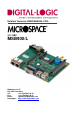
Detailed Technical USER MANUAL FOR: 3.5”-SBC MSB900/L Nordstrasse 11/F CH- 4542 Luterbach Tel.: ++41 (0)32 681 58 00 Fax: ++41 (0)32 681 58 01 Email: support@digitallogic.com Homepage: http://www.digitallogic.
DIGITAL-LOGIC AG MSB900/L Detailed Technical Manual V1.0 For internal use only: File: Path: MSB900_Detailed_V1.0 R:\HANDBUCH\MSB\MSB900\MSB900_Detailed_V1.0.doc COPYRIGHT 2008 BY DIGITAL-LOGIC AG This publication is protected by copyright and all rights are reserved.
DIGITAL-LOGIC AG MSB900/L Detailed Technical Manual V1.0 Table of Contents 1. Preface.......................................................................................................................5 1.1. 1.2. 1.3. 1.4. 1.5. 1.6. 1.7. 1.8. 1.9. 1.10. 1.11. Trademarks ................................................................................................................... 5 Disclaimer ........................................................................................................
DIGITAL-LOGIC AG 5.6.3. 5.6.4. 5.6.5. 5.7. 5.8. Watchdog ................................................................................................................................... 28 ROM-BIOS Sockets ................................................................................................................... 28 BIOS CMOS Setup .................................................................................................................... 29 CMOS RAM Map.................................
DIGITAL-LOGIC AG MSB900/L Detailed Technical Manual V1.0 1. PREFACE The information contained in this manual has been carefully checked and is believed to be accurate; it is subject to change without notice. Product advances mean that some specifications may have changed. DIGITAL-LOGIC AG assumes no responsibility for any inaccuracies, or the consequences thereof, that may appear in this manual.
DIGITAL-LOGIC AG 1.5. MSB900/L Detailed Technical Manual V1.0 Recycling Information All components within this product fulfill the requirements of the RoHS (Restriction of Hazardous Substances Directive). The product is soldered with a lead free process. 1.6. Technical Support 1. Contact your local DIGITAL-LOGIC Technical Support, in your country. 2. Use the Internet Support Request form at http://support.digitallogic.
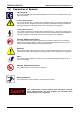
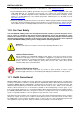
DIGITAL-LOGIC AG 1.8. MSB900/L Detailed Technical Manual V1.0 Explanation of Symbols CE Conformity This symbol indicates that the product described in this manual is in compliance with all applied CE standards. Caution, Electric Shock! This symbol and title warn of hazards due to electrical shocks (> 60V) when touching products or parts of them. Failure to observe the precautions indicated and/or prescribed by the law may endanger your life/health and/or result in damage to your equipment.
DIGITAL-LOGIC AG 1.9. MSB900/L Detailed Technical Manual V1.0 Applicable Documents and Standards The following publications are used in conjunction with this manual. When any of the referenced specifications are superseded by an approved revision, that revision shall apply. All documents may be obtained from their respective organizations. Advanced Configuration and Power Interface Specification Revision 2.
DIGITAL-LOGIC AG MSB900/L Detailed Technical Manual V1.0 Smart Battery Data Specification Revision 1.1, December 11, 1998. www.sbs-forum.org System Management Bus (SMBus) Specification Version 2.0, August 3, 2000 Copyright © 1994, 1995, 1998, 2000 Duracell, Inc., Energizer Power Systems, Inc., Fujitsu, Ltd., Intel Corporation, Linear Technology Inc., Maxim Integrated Products, Mitsubishi Electric Semiconductor Company, PowerSmart, Inc., Toshiba Battery Co. Ltd.
DIGITAL-LOGIC AG MSB900/L Detailed Technical Manual V1.0 RoHS is often referred to as the "lead-free" directive but it restricts the use of the following substances: Lead Mercury Cadmium Chromium VI PBB and PBDE The maximum allowable concentration of any of the above mentioned substances is 0.1% (except for Cadmium, which is limited to 0.01%) by weight of homogeneous material.
DIGITAL-LOGIC AG MSB900/L Detailed Technical Manual V1.0 1.12. Swiss Quality 100% Made in Switzerland DIGITAL-LOGIC is a member of "Swiss-Label" This product was not manufactured by employees earning piecework wages This product was manufactured in humane work conditions All employees who worked on this product are paid customary Swiss market wages and are insured ISO 9000:2001 (quality management system) 1.13.
DIGITAL-LOGIC AG MSB900/L Detailed Technical Manual V1.0 2. OVERVIEW 2.1. Standard Features of the MSB900/L The MICROSPACE 3.5”-SBC is a miniaturized modular device incorporating the major elements of a PC/AT compatible computer. It includes standard PC/AT compatible elements, such as: 2.2.
DIGITAL-LOGIC AG 2.3. MSB900/L Detailed Technical Manual V1.
DIGITAL-LOGIC AG 2.4. MSB900/L Detailed Technical Manual V1.0 MSB900/MSB900L specifications CPU CPU CPU Core Supply Mode Compatibility Word Size Secondary Cache Physical Addressing Virtual Addressing Clock Rates Socket Standard Specification GEODE LX900 1.
DIGITAL-LOGIC AG MSB900/L Detailed Technical Manual V1.0 Mass Storage FD HD Specification Floppy disk interface not supported E-IDE interface, AT-type, for max. 2 hard disks, 44pin connector, for 1.3, 1.8 and 2.5" hard disk with 44 pins IDE Standard AT Interfaces: SuperIO Chip Parallel Keyboard Mouse Speaker RTC Backup current RTC-backup MSB900 RTC-backup MSB900L Specification Name FIFO IRQs Addr. Standard Option COM1 yes IRQ4 3F8 RS232C COM2 yes IRQ3 2F8 RS232C COM1/2 available on headers onboard.
DIGITAL-LOGIC AG Operating Environment Relative humidity Vibration Shock Temperature MSB900/L Detailed Technical Manual V1.0 Specification 5-90%, non-condensing 5-2000Hz, 0.
DIGITAL-LOGIC AG 2.7. 2.7.1. MSB900/L Detailed Technical Manual V1.0 Dimensions & Diagrams MSB900/L Board / Version MSB900/L Unit: mm (millimeter) Tolerance: + / - 0.1mm 17 Date / Author 25.10.
DIGITAL-LOGIC AG MSB900/L Detailed Technical Manual V1.
DIGITAL-LOGIC AG MSB900/L Detailed Technical Manual V1.
DIGITAL-LOGIC AG MSB900/L Detailed Technical Manual V1.
DIGITAL-LOGIC AG 2.7.2. MSB900/L Detailed Technical Manual V1.0 MSB800CON Part Nr 802205 Board / Version MSB800CON Unit: mm (millimeter) Tolerance: + / - 0.1mm 21 Date / Author 25.10.
DIGITAL-LOGIC AG 2.8. MSB900/L Detailed Technical Manual V1.0 MSB900/L Incompatibilities to a standard PC/AT None. 2.9. Related Application Notes Application Notes are available at http://www.digitallogic.com support, or on any DIGITAL-LOGIC Application CD. # Description 2.10. High Frequency Radiation (to meet EN55022) All connectors are filtered onboard to comply with the EMI standards.
DIGITAL-LOGIC AG MSB900/L Detailed Technical Manual V1.0 2.11. Battery-Lifetime Battery specs: Lowest temp. -40°C Nominal temp. +20°C Highest temp. +85°C 400mAh 3.6V 350mAh Ca. 3.6V VCC (+5) switched ON µA <1 VCC (+5V) switched off µA <3 >3.5 years >3.5 year Manufacturer: pba Type: ER10280 Capacity versus Temp: 10uA 420mAh Voltage versus Temp. 10uA 3.6V Nominal values: 3.6V / 400mAh @ 0.5mA / -55°C...
DIGITAL-LOGIC AG MSB900/L Detailed Technical Manual V1.0 4. BIOS HISTORY This BIOS history is for the MSB900/L. This BIOS history is not for the following products: MSEP900, MSM900, SM900 Version: 1.23 Date: 02.2007 Status: Initial Release Modifications: - Note… This product has a unique BIOS version. For a description of the other features of the BIOS, please refer to the driver/software/BIOS manual “GEODE_LX800-LX900” on the Product CD.
DIGITAL-LOGIC AG MSB900/L Detailed Technical Manual V1.0 5. DETAILED SYSTEM DESCRIPTION This system configuration is based on the ISA architecture. Check the I/O and memory map in this chapter. 5.1. Power Requirements The power is connected through the wide-range power connector. The supply uses only the +8V to +32V and the ground connection. Attention: Make sure the power plug is wired correctly before supplying power to the board! A built-in diode protects the board against reverse polarity.
DIGITAL-LOGIC AG 5.3. MSB900/L Detailed Technical Manual V1.0 CPU, Boards and RAMs 5.3.1. CPUs of this MICROSPACE Product Processor: GEODE LX900 5.3.2. Type: National Clock: 600 MHz Numeric Coprocessor It is integrated in the LX900 CPU. 5.3.3. DDRAM Memory Speed: Size: Bits: Capacity: Bank: 5.4. 5.4.1. 333 DDR-SODIMM DDRDIMM 200pin 64bit 256-1024MBytes DDR-SODIMM 1 Interfaces Keyboard AT compatible and PS/2 Mouse The PS/2 Keyboard and Mouse are combined on the PS2-connector.
DIGITAL-LOGIC AG 5.4.3. MSB900/L Detailed Technical Manual V1.0 Serial Ports COM1-COM2 The serial channels are fully compatible with 16C550 UARTS. COM1 is the primary serial port, and is supported by the board's ROM-BIOS as the PC-DOS 'COM1' device. The secondary serial port is COM2; it is supported as the 'COM2' device.
DIGITAL-LOGIC AG 5.6. 5.6.1. MSB900/L Detailed Technical Manual V1.0 Timers and Counters Programmable Timers An 8253 compatible timer/counter device is also included in the board's ASIC device. This device is utilized in precisely the same manner as in a standard AT implementation. Each channel of the 8253 is driven by a 1.190 MHz clock, derived from a 14.318 MHz oscillator, which can be internally divided in order to provide a variety of frequencies.
DIGITAL-LOGIC AG 5.6.4.1. Standard BIOS ROM Device: FWH Map: E0000 - FFFFFh C0000 - C7FFFh CC000 - CFFFFh 5.6.5. MSB900/L Detailed Technical Manual V1.0 Core BIOS 128k VGA BIOS 32k FREE BIOS CMOS Setup If wrong setups are memorized in the CMOS-RAM, the default values will be loaded after resetting the RTC/CMOS-RAM by de-soldering the battery. If the battery is down, it is always possible to start the system with the default values from the BIOS. 5.7.
DIGITAL-LOGIC AG MSB900/L Detailed Technical Manual V1.
DIGITAL-LOGIC AG MSB900/L Detailed Technical Manual V1.0 CMOS Map continued... Location Description 0Eh CMOS Location for Bad CMOS and Checksum Flags Bit 7 = Flag for CMOS Lost Power 0 1 Bit 6 = = Power OK Lost Power = Flag for CMOS checksum bad 0 1 = = Checksum is valid Checksum is bad 0Fh Shutdown Code 10h Diskette Drives Bits 7-4 = Diskette Drive A 0000 0001 0010 0011 0100 0101 = = = = = = Not installed Drive A = 360 kB Drive A = 1.2MB Drive A = 720 kB Drive A = 1.44MB Drive A = 2.
DIGITAL-LOGIC AG MSB900/L Detailed Technical Manual V1.0 CMOS Map continued...
DIGITAL-LOGIC AG MSB900/L Detailed Technical Manual V1.0 CMOS Map continued...
DIGITAL-LOGIC AG MSB900/L Detailed Technical Manual V1.0 CMOS Map continued... Location Description 33h Base Memory Installed Bit 7 = Flag for Memory Size 0 1 = = 640kB 512kB Bits 6-0 = Reserved 34h Minor CPU Revision Differentiates CPUs within a CPU type (i.e., 486SX vs 486 DX, vs 486 DX/2). This is crucial for correctly determining CPU input clock frequency. During a power-on reset, Reg DL holds minor CPU revision. 35h Major CPU Revision Differentiates between different CPUs (i.e.
DIGITAL-LOGIC AG 5.8.1. MSB900/L Detailed Technical Manual V1.0 EEPROM Memory for Setup The EEPROM is used for setup and configuration data, stored as an alternative to the CMOS-RTC. Optionally, the EEPROM setup driver may update the CMOS RTC, if the battery is running down and the checksum error would appear and stop the system. The capacity of the EEPROM is 2 kByte.
DIGITAL-LOGIC AG 5.9.2. MSB900/L Detailed Technical Manual V1.0 System I/O map The following table details the legacy I/O range for 000h through 4FFh. Each I/O location has a read/write (R/W) capability. Note the following abbreviations: --- Unknown or can not be determined. Yes Read and write the register at the indicated location. No shadow required. WO Write only. Value written can not be read back. Reads do not contain any useful information. RO Read only. Writes have no effect.
DIGITAL-LOGIC AG MSB900/L Detailed Technical Manual V1.0 I/O Map Continued… I/O Addr. Function Size R/W Comment If KEL Memory Offset 100h[0] = 1(EmulationEnabled bit). 060h Keyboard/Mouse - Data Port 8bit Yes 061h Port B Control 8bit Yes --- --- 062h-063h No Specific Usage 064h Keyboard/Mouse - Command/ Status 8bit 065h-06Fh No Specific Usage --- If MSR 5140001Fh[0] = 1 (SNOOP bit) and KEL Memory Offset 100h[0] = 0 (EmulationEnabled bit).
DIGITAL-LOGIC AG MSB900/L Detailed Technical Manual V1.0 I/O Map Continued… I/O Addr. Function Size R/W Comment 0CCh Master DMA Address - Channel 7 8bit Yes 16bit values in two transfers.
DIGITAL-LOGIC AG MSB900/L Detailed Technical Manual V1.0 I/O Map Continued… I/O Addr. Function Size R/W Comment 3F1h Floppy Status R B 8bit RO First Floppy. 3F2h Floppy Digital Out 8bit Shw@ First Floppy. 3F3h No Specific Usage 8bit 3F4h Floppy Cntrl Status 8bit RO First Floppy. 3F5h Floppy Data 8bit Yes First Floppy.
DIGITAL-LOGIC AG MSB900/L Detailed Technical Manual V1.0 6. VGA 6.1. VGA/LCD Controller of the Geode LX900 • Highly integrated flat panel and CRT GUI Accelerator & Multimedia Engine, Palette/DAC, Clock Synthesizer, and integrated frame buffer • HiQColor TM Technology implemented with TMED (Temporal Modulated Energy Distribution) • Hardware Windows Acceleration • Hardware Multimedia Support • High-Performance flat panel display resolution and color depth at 3.
DIGITAL-LOGIC AG MSB900/L Detailed Technical Manual V1.0 7. VIDEO INPUT The MSB900 contains a low-cost video input port. It consist of LX900’s video input port (VIP) and the external frame grabber chip SAA7111A. This port is capable of digitizing a CVBS video signal with 15 frames per second at a resolution of 352x288bits. Note that this frame rate is only achievable when the raw data stream is compressed before being stored on the hard drive.
DIGITAL-LOGIC AG MSB900/L Detailed Technical Manual V1.
DIGITAL-LOGIC AG MSB900/L Detailed Technical Manual V1.
DIGITAL-LOGIC AG X1 Power Supply Pin 1 (Shield) 2 3 X14 Pin 1 MSB900/L Detailed Technical Manual V1.
DIGITAL-LOGIC AG X15 MSB900/L Detailed Technical Manual V1.0 Operator Panel / Flat Panel (bottom side) X15 is intended to be used internally to attach an operator panel. Some signals may not be present or are shared with other connectors. This connector is not assembled and is only for OEM-specific applications. A 2mm x 44pin header is needed.
DIGITAL-LOGIC AG X15 MSB900/L Detailed Technical Manual V1.0 Reverse Pin Configuration MSB900 LVDS X15 (on component side) Attention! When X15 is soldered on the component side, a different pin numbering schema must be applied. Odd and even pin numbers are swapped.
DIGITAL-LOGIC AG X31 MSB900/L Detailed Technical Manual V1.
DIGITAL-LOGIC AG X39 MSB900/L Detailed Technical Manual V1.
DIGITAL-LOGIC AG X52 Pin 1 2 3 4 5 MSB900/L Detailed Technical Manual V1.0 USB UDOC (not assembled) Signal VCC NC USB-P2NC USB-P2+ Pin 6 7 8 9 10 Signal NC GND NC NC NC Attention! X52 for USB-DOC-Flash drives are only for OEM use. The connector is not assembled. The UDOC may be assembled if the CompactFlash is not assembled.
DIGITAL-LOGIC AG X61 MSB900/L Detailed Technical Manual V1.
DIGITAL-LOGIC AG MSB900/L Detailed Technical Manual V1.0 X101 PCI-104 BUS Interface Pin 1 2 3 4 5 6 7 8 9 10 11 12 13 14 15 16 17 18 19 20 21 22 23 24 25 26 27 28 29 30 A GND/5.0V KEY2 VI/O AD05 C/BE0* GND AD11 AD14 +3.3V SERR* GND STOP* +3.3V FRAME* GND AD18 AD21 +3.3V IDSEL0 AD24 GND AD29 +5V REQ0* GND GNT1* +5V CLK2 GND +12V -12V B Reserved AD02 GND AD07 AD09 VI/O AD13 C/BE1* GND PERR* +3.3V TRDY* GND AD16 +3.
DIGITAL-LOGIC AG MSB900/L Detailed Technical Manual V1.0 X230 JTAG-Port Pin 1 3 Signal TCK TDI Pin Signal 2 TMS 4 TDO X301 VGA Monitor (CRT-Signals) 15pins High-Density DSub Pin Signal 1 Red 2 Green 3 Blue 13 H-Synch 14 V-Synch 5 + 11 Bridged 5, 6, 7, 8 Grounded The VGA-CRT signals from J2 must be wired to a standard VGA High Density DSub-connector (female): The LCD signals must be wired panel-specific.
DIGITAL-LOGIC AG MSB900/L Detailed Technical Manual V1.0 9. JUMPER LOCATIONS ON THE BOARD The following figure shows the location of all jumper blocks on the MSB900/L board. The numbers shown in this figure are silk screened on the board so that the pins can easily be located. This chapter refers to the individual pins for these jumpers. The default jumper settings are indicated with asterisks. Be careful: some jumpers are soldering bridges; you will need a miniature soldering station with a vacuum pump.
DIGITAL-LOGIC AG MSB900/L Detailed Technical Manual V1.
DIGITAL-LOGIC AG MSB900/L Detailed Technical Manual V1.0 10.CABLE INTERFACES 10.1. The Hard Disk Cable 44pin IDT Terminal for Dual Row (2.00mm grid) and 1.00mm flat cable; 44pins = 40pins signal and 4pins power. 1 2 39 1 2 40 39 43 44 40 43 44 Max. length for the IDE cable is 30cm. Attention! Check the pin 1 marker of the cable and the connector before you power-on.
DIGITAL-LOGIC AG MSB900/L Detailed Technical Manual V1.0 10.2. The COM1/LPT Serial Interface Cable Terminal for dual row 2mm grid and 1mm flat cable.
DIGITAL-LOGIC AG MSB900/L Detailed Technical Manual V1.0 10.3. The COM2 Serial Interface Cable DT terminal for dual row 0.1" (2.54mm grid) and 1.27mm flat cable. Connector X39 Pin Pin 1 Pin 2 Pin 3 Pin 4 Pin 5 Pin 6 Pin 7 Pin 8 Pin 9 Pin 10 Signal = DCD = DSR = RXD = RTS = TXD = CTS = DTR = RI = GND COM2 9pin D-Sub male 1 6 2 7 3 8 4 9 5 Attention! • Do not short circuit these signal lines. • Never connect any pins on the same plug or to any other plug on the MICROSPACE MSB900/L.
DIGITAL-LOGIC AG MSB900/L Detailed Technical Manual V1.0 11. THERMAL SPECIFICATIONS 11.1. Thermal Analysis for Case Integration The MSB900/L has a unique thermal design. Heat sources are located on the bottom side of the PCB. Usually this means the board will be mounted upside down with the CPU thermally in contact with a heat sink. Alternatively, the CPU will be in contact with the system enclosure which then works as a heat sink. The LX900 CPU is rated with a Total Dissipated Power (TDP) of 3.
DIGITAL-LOGIC AG MSB900/L Detailed Technical Manual V1.0 12.ASSEMBLY VIEWS 12.1.
DIGITAL-LOGIC AG MSB900/L Detailed Technical Manual V1.
DIGITAL-LOGIC AG MSB900/L Detailed Technical Manual V1.0 12.2. Mechanical Dimensions MSB900 Version Unit: mm (millimeter) Tolerance: +/- 0.1mm Date: 28.03.
DIGITAL-LOGIC AG MSB900/L Detailed Technical Manual V1.0 13.PXE-BOOT AND PXE-SETUP IN THE BIOS PXE Protocol PXE is defined on a foundation of industry-standard Internet protocols and services that are widely deployed in the industry, namely TCP/IP, DHCP, and TFTP. These standardize the form of the interactions between clients and servers.
DIGITAL-LOGIC AG MSB900/L Detailed Technical Manual V1.0 BIOS-Setup Screen with the LAN-BOOT (PXE) DISABLE / ENABLE menu: After ENABLING the LAN-Boot, the Password must be entered. The Password must be requested with the PXE-licence order form on the following page.
DIGITAL-LOGIC AG MSB900/L Detailed Technical Manual V1.0 14.PXE-LICENSE ORDER The PXE-Function must be licensed before it can be enabled. To order, fill out and sign this form; return to the fax number below. This form may be printed out separately from the digital copy of this manual on the Product CD. Note... One license per form Each computer system requires an individual, one-time royalty payment for the PXE-license.
DIGITAL-LOGIC AG MSB900/L Detailed Technical Manual V1.0 15.
DIGITAL-LOGIC AG RoHS Commitment ROM-BIOS RTC MSB900/L Detailed Technical Manual V1.