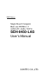
SBC Series Single Board Computer Half-size PICMG 1.3 with LAN, Audio, SATA SEH-9450-LAS User’s Manual CONTEC CO.,LTD.
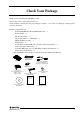
Check Your Package Thank you for purchasing the CONTEC product. The product consists of the items listed below. Check, with the following list, that your package is complete. contact your retailer.
Copyright Copyright 2007 CONTEC CO., LTD. ALL RIGHTS RESERVED No part of this document may be copied or reproduced in any form by any means without prior written consent of CONTEC CO., LTD. CONTEC CO., LTD. makes no commitment to update or keep current the information contained in this document. The information in this document is subject to change without notice. All relevant issues have been considered in the preparation of this document.
Table of Contents Check Your Package ................................................................................................................................ i Copyright .................................................................................................................................................ii Trademarks ..............................................................................................................................................ii Caution about Battery.........
System FAN Connector: FAN2 .............................................................................................................15 Front Panel Connector: FP1............................................................................................................16 Power Switch (Power BT) ..............................................................................................................16 Reset Switch (RESET)...............................................................................
8. BIOS SETUP 37 Introduction............................................................................................................................................ 37 Starting Setup ................................................................................................................................. 37 Using Setup..................................................................................................................................... 38 Getting Help ...........................
vi SEH-9450-LAS
1. Introduction 1. Introduction About the SBC This product is a half-size sized single-board computer that supports PICMG1.3. It uses Intel (R) 945GME Chipset. The supported CPU is Intel (R) Core Duo / Core 2 Duo processor. For the memory, up to 4 GB (total capacity : 3.1GB) of DDR2 SDRAM can be mounted. The all-in-one design features a wide variety of interfaces including Analog RGB, LVDS, SDVO, USB2.0 x 4, SATA x 2, 1000BASE-T/100BASE-TX, audio, IDE, serial and PS/2 Keyboard/Mouse.
1. Introduction Customer Support CONTEC provides the following support services for you to use CONTEC products more efficiently and comfortably. Web Site Japanese English Chinese http://www.contec.co.jp/ http://www.contec.com/ http://www.contec.com.cn/ Latest product information CONTEC provides up-to-date information on products. CONTEC also provides product manuals and various technical documents in the PDF.
1. Introduction Safety Precautions Understand the following definitions and precautions to use the product safely. Safety Information This document provides safety information using the following symbols to prevent accidents resulting in injury or death and the destruction of equipment and resources. Understand the meanings of these labels to operate the equipment safely. DANGER DANGER indicates an imminently hazardous situation which, if not avoided, will result in death or serious injury.
1. Introduction Environments Use this product in the following environment. If used in an unauthorized environment, the board may overeat, malfunction, or cause a failure. Operating temperature 0 - 60°C Operating humidity 10 - 90%RH (No condensation) Corrosive gases None Floating dust particles Not to be excessive Inspection Inspect the product periodically as follows to use it safely. - Check that the board has no dust or foreign matter adhering.
2. System Reference 2. System Reference Specification Table 2.1. Functional Specifications < 1 / 2 > Type Specifications Supported CPU Intel(R) Core Duo / Core 2 Duo (FSB 533 / 667 MHz) Cache Built in CPU Processor socket Socket M Memory (Option) Up to MAX 4G, DDR2 400 / 533 / 667, 200 pin SO-DIMM Socket X 2 *1 Chipset Intel(R) 945GME+ ICH7M-DH BIOS Phoenix AwardBIOS, PnP support VGA Built in Intel 945GME, One Analog RGB D-Sub 15pin connector.
2. System Reference Table 2.1. Functional Specifications < 2 / 2 > Type Watchdog Timer Specifications Software programmable 255 levels (1 - 255sec). When time up: Reset General-purpose I/F None Hardware Monitor Monitoring of the temperature of CPU and board, power supply voltage, and fan speed RTC The coin type Lithium battery specification is shown in table Specification CR2450 Voltage 3V Capacity 620mAh Weigh 6.3g * Backup time: Over 7 years at 25ºC.
2. System Reference Power Management Features - Support both ACPI (Advanced Configuration and Power Interface) and legacy (APM) power management. - ACPI v2.0 compliant - APM v1.
2. System Reference Connector & Jumper Location Top side COM1 COM2 JCOM1 SATA1 SATA2 FAN1 FP1 IDE1 AUDIO1 TPM1 JP1 USB1 LAN1 USB2 USB3 VGA1 PWR1 KB/MS1 FAN2 SDVO1 LVDS1 LVDS2 JBAT1 Bottom side CF1 DIMM1 DIMM2 PCI1 Figure 2.1.
2. System Reference Table 2.3.
2. System Reference Block Diagram IMVP6 ISL6262CR CK-410M ISC954226 CPU Socket for Yonah & Merom DATA R.G.B. CTRL ADDR R.G.B. D-SUB 15Pin Channel A GMCH DDR2 667 Dual-Channel 945GME LVDS 18bit 2Channel Channel B LVDS BUS DMA33/66/100 USB 2.0 USB Interface PICMG 1.3 BUS ICH7M-DH Mini PCI PCI Interface AC LINK SATA Conncetor SATA Interface LPC IO W83627EHG LPC BUS Audio Codec ALC202A Keyboard & Mouse LAN PHY 10/100 b/s 82562GZ GIGA LAN 82573 PICMG 1.
3. Hardware Installations 3. Hardware Installations This chapter provides information on how to use the jumpers and connectors on the product in order to set up a workable system. Installation procedure (1) Confirm the power supply is off. (2) Install the processor with correct orientation. (3) Mount the Heat sink on the top of the processor. (The heat sink with a fan connects a fan cable to the fan connector on a board.) (4) Insert the DDR2 SDRAM module with correct orientation.
3. Hardware Installations CPU Installation: This product supports a single Intel socket-M type Core Duo processor or Core 2 Duo processor. The processor’s VID pins automatically program the voltage regulator on the CPU card to the required processor voltage. The host bus speed is automatically selected. The processor connects to the CPU card through the socket M. The socket-M comes with a turn lock to secure the processor.
3. Hardware Installations Audio Connector: AUDIO1 This connector connects the Audio jack cable. Table 3.2. Audio Connector AUDIO1 10 2 9 1 PIN No. Function PIN No. Function 10 LINE-IN-L 9 LINE-IN-R GND 8 GND 7 6 MICIN 5 NC 4 GND 3 GND 2 LINE-OUT-L 1 LINE-OUT-R Compact Flash Slot: CF1 This product provides a Compact Flash interfaces. This interface is a very small removable mass storage device. It provides compatibility plus True IDE functionality compatible with ATA/ATA-4.
3. Hardware Installations Serial Port Connector: COM1 / COM2 Serial 1 (COM1), Serial 2 (COM2), are onboard serial ports of the product. The following table shows the pin assignments of these connectors. Table 3.4. Serial Port Connector PIN No. RS-232C RS-422 RS-485 1 2 3 4 5 6 7 8 9 10 DCD RXD TXD DTR GND DSR RTS CTS RI N.C. TXTX+ RX+ RXGND N.C. N.C. N.C. N.C. N.C. TXTX+ RX+ RXGND N.C. N.C. N.C. N.C. N.C.
3. Hardware Installations CPU FAN Connector: FAN1 FAN1 is a 4-pins box-header for the CPU cooling fan power connector. The fan must be a 12V fan. Pin 3 is for Fan tachometer input. Pin is for PWM Fan output control. Pin 2 is for 12V voltage. Table 3.5. CPU FAN Connector PIN No. FAN1 4 3 2 1 1 Function GND 2 POWER 3 FAN Sense 4 PWM FAN control Housing: 5102-04 (molex) Contact: 5104 (molex) System FAN Connector: FAN2 FAN2 is a 3-pins box-header for the CPU cooling fan power connector.
3. Hardware Installations Front Panel Connector: FP1 FP1 consist of header can be connected to a front panel power switch. includes headers for these I/O connections: The front panel connector Power Switch (Power BT) This header can be connected to a power push switch for ATX power supply. Reset Switch (RESET) This header can be connected to a reset push switch. Power LED This header can be connected to an LED that will light when the computer is powered on.
3. Hardware Installations IDE port Connector: IDE1 This product provides a bus-mastering PCI IDE interface. This interface support PIO Mode 3, PIO Mode 4, ATAPI devices (e.g., CD-ROM), and Ultra DMA/33/66/100 synchronous-DMA mode transfers. The BIOS supports logical block addressing (LBA) and extended cylinder head sector (ECHS) translation modes. The BIOS automatically detects the IDE device transfer rate and translation mode.
3. Hardware Installations Keyboard / Mouse Connector: KB/MS1 The CPU card provides a standard PS/2 keyboard/mouse connector for attaching a PS/2 keyboard/mouse. You will connect with an add-on cable for a PS/2 keyboard/mouse. You can select that plug a PS/2 mouse directly, PS/2 keyboard directly or both (use Y-cable) by jumper setting. The PS2 Connector pin definition is shown below: Table 3.9. Keyboard / Mouse Connector (KB/MS1) PIN No.
3. Hardware Installations LVDS LCD Connector: LVDS1 / LVDS2 LVDS1 and LVDS2 consist of 30-pin and 20-pin connectors that using the Hirose’s DF13A-30DP-1.25V /DF13A-20DP-1.25V. The SEH-9450-LAS supports 2 channels (2 x 18-bit) of LVDS LCD panel display. Table 3.11. LVDS Connector LVDS1 30 2 29 1 PIN No. Function PIN No. Function 2 4 6 8 10 12 14 16 18 20 22 24 26 28 30 TXL1+ TXL1GND N.C. N.C. GND+3.3V +3.
3. Hardware Installations Mini PCI type III expansion socket: PCI1 The Mini PCI specification defines an alternate implementation for small form factor PCI card. Table 3.12. Mini PCI socket Pin No. Signal name 1 TIP Pin No. Signal name 2 Key RING Key Pin No. Signal name Pin No. Signal name 63 3.3V 64 FRAME# 65 CLKRUN# 66 TRDY# STOP# 3 8PMJ-3 4 8PMJ-1 67 SERR# 68 5 8PMJ-6 6 8PMJ-2 69 GND 70 3.
3. Hardware Installations Power supply Connector: PWR1 Table3.13. Power supply connector PWR1 3 1 4 2 PIN No. Function PIN No. Function 3 +12V 1 GND 4 +12V 2 GND Suitable Housing: 39-01-2200 (Correpond) Suitable: Contact: 5556 (correspond) Maker: Molex Serial ATA Connector: SATA1 / SATA2 Serial ATA is the revolutionary ATA interface that provides scalable performance for IDE device.
3. Hardware Installations Serial Digital Video Output: SDVO1 The SDVO specification defines an alternate implementation for PCI express card. are as follows: Table 3.15. SDVO1 Connector PIN No. Function 2 SDVOB_GREEN4 SDVOB_GREEN+ 6 GND 8 SDVOB_CLK10 SDVOB_CLK+ SDVO1 12 GND 30 2 14 SDVOB_INT16 SDVOB_INT+ 29 1 18 GND 20 PCIRST22 GPIO21 24 NC 26 +3.3V 28 LVDS_OUT 30 LVDS_IN Note: PCIe X16 SDVO PORT Can’t use at same time 22 The pin assignments PIN No.
3. Hardware Installations USB Connector: USB1, USB2, USB3 This product have four USB (v2.0 compliant) ports. One box-header connector USB1. This box-header connector is for the optinal USB cable to provide two A Type connectors; and two USB A Type connectors. Table 3.16. USB Pin-header Connector USB1 10 8 6 4 2 9 7 5 3 1 Pin No. Function Pin No. Function 10 N. C. 9 N. C. 8 GND 7 GND 6 USB1+ 5 USB0+ 4 USB1- 3 USB0- 2 VCC1 1 VCC0 * Optional USB Cable: USB Connector Cable Table 3.
3. Hardware Installations VGA Connector: VGA1 This is a VGA connector (D-Sub 15 pin). The pin assingnment is shown below. Table 3.18. VGA Connector VGA1 6 1 11 5 15 10 PIN No. 24 Function PIN No. Function 1 RED 9 N.C 2 GREEN 10 GND 3 BLUE 11 D-DATE 4 N.C 12 N.
4. Jumper Setting 4. Jumper Setting Clear CMOS Content & BIOS setting cancel: JBAT1 The time, date, and CMOS values can be specified in the Setup program. The CMOS values can be returned to their defaults by using the Setup program. The RAM data contains the password information is powered by the onboard button cell battery. User can erase the CMOS memory content by short pin2 and pin3 of JBAT1 together. Table 4.1.
4. Jumper Setting CF Master / Slave selector: JP1 On board CF slot is connected to Secondary IDE. card. Usually, please use it with a master setup. Table 4.3. This jumper is select Master/Slave of CF memory CF Master / Slave selector JP1 Function 1 2 3 Set to Master 1 2 3 Set to Slave (Default) RS-232/422/485 Selector: JCOM1 Table 4.4.
4. Jumper Setting Setting the RS-422/RS-485 receiver disable control jumper When the RS-422/RS-485 port is used, the RTS signal is used for driver enable control Connecting JCOM1 Pins 14 and 16 disables the receiver at the same time, preventing the port from receiving output data to an external device. RS-422/485 setting 4.7KΩ RTS# 4.7KΩ 4.7KΩ 4.7KΩ 4.7KΩ JCOM1: 14-6 6.2ΚΩ R 1ΚΩ 4.7KΩ JCOM1: 15-6 SOUTB 6.2ΚΩ 10 5 D 6 Figure 4.1.
4.
5. CPU Board Resources 5. CPU Board Resources System address map The GMCH memory map includes a number of programmable ranges. All of these ranges must be unique and non-overlapping. There are no hardware interlocks to prevent problems in the case of overlapping ranges. Accesses to overlapped ranges may produce indeterminate results.
5.
6. Watch-Dog-Timer (WDT) Setting 6. Watch-Dog-Timer (WDT) Setting Introduction The watchdog timer serves as a safeguard against possible system lock-up in your industrial computer system. In most industrial environments, there are heavy equipment, generators, high-voltage power lines, or power drops that have adverse effects on your computer system. For instance, when a power drop occurs, it could cause the CPU to come to a halt state or enter into an infinite loop, resulting in a system lock-up.
6. Watch-Dog-Timer (WDT) Setting (2) Example programming The following example is written in Intel8086 assembly language.
6.
6.
7. Hardware Monitor 7. Hardware Monitor Hardware Monitor Hardware Monitor function is included in Hardware Monitor controller (Winbond W83627HF) on this product. You can read Temperature, Voltage and Fan Sensor output of SBC. Temperature Two Thermistor are mounted on SBC as following. You can read Temperature of this position. Voltage You can read +3.3V, +5V, +1.05, +1.8V, +1.5V, 5VSB, Vcore of SBC. VTT(1.
7.
8. BIOS Setup 8. BIOS Setup Introduction This chapter discusses Award’s Setup program built into the FLASH ROM BIOS. The Setup program allows users to modify the basic system configuration. This special information is then stored in battery-backed RAM so that it retains the Setup information when the power is turned off. The rest of this chapter is intended to guide you through the process of configuring your system using Setup.
8. BIOS Setup Using Setup In general, you use the arrow keys to highlight items, press to select, use the PageUp and PageDown keys to change entries, press for help and press to quit. The following table provides more detail about how to navigate in the Setup program using the keyboard. Table 8.1.
8. BIOS Setup Main Menu Once you enter the Award BIOS CMOS Setup Utility, the Main Menu will appear on the screen. The Main Menu allows you to select from several setup functions and two exit choices. Use the arrow keys to select among the items and press to accept and enter the sub-menu. Note that a brief description of each highlighted selection appears at the bottom of the screen. Figure 8.1. Main Manu Setup Items The main menu includes the following main setup categories. all entries.
8. BIOS Setup PnP / PCI Configuration This entry appears if your system supports PnP / PCI. Load Fail-Safe Defaults Use this menu to load the BIOS default values for the minimal/stable performance for your system to operate. Load Optimized Defaults Use this menu to load the BIOS default values that are factory settings for optimal performance system operations. While Award has designed the custom BIOS to maximize performance, the factory has the right to change these defaults to meet their needs.
8. BIOS Setup Standard CMOS Setup Figure 8.2. Standard CMOS Setup The items in Standard CMOS Setup Menu are divided into 10 categories. Each category includes no, one or more than one setup items. Use the arrow keys to highlight the item and then use the or keys to select the value you want in each item.
8. BIOS Setup Main Menu Selections This table shows the selections that you can make on the Main Menu Table 8.2. Main Menu Selections Item Options Description Set the system date.
8. BIOS Setup IDE Adapters The IDE adapters control the hard disk drive. drive. Use a separate sub menu to configure each hard disk Use the legend keys to navigate through this menu and exit to the main menu. Use Table 3 to configure the hard disk. Table 8.3. IDE Adapters configurations Item Options Description Press Enter to auto-detect the HDD on this channel. If detection is successful, it fills the remaining fields on this menu.
8. BIOS Setup Advanced BIOS Features Setup This section allows you to configure your system for basic operation. You have the opportunity to select the system’s default speed, boot-up sequence, keyboard operation, shadowing and security. Figure 8.3.
8. BIOS Setup CPU Feature Figure 8.4. CPU Feature Setup Press to configure the settings relevant to CPU Feature. Table 8.4. CPU Features Selections Description Choice Delay Prior to Thermal Select the interval to setup the delay timer for CPU Thermal-Throuttling C1E Function CPU C1E Function Select.
8. BIOS Setup Description Choice Execute Disable Bit When disabled, forces the XD feature flag to always return 0. Hard Disk Boot Priority Figure 8.5. Hard Disk Boot Priority Setup With the field, there is the option to choose, aside from the hard disks connected, “Bootable add-in Cards” which refers to other external device.
8. BIOS Setup Virus Warning When enabled, you receive a warning message if a program (specifically, a virus) attempts to write to the boot sector or the partition table of the hard disk drive. You should then run an anti-virus program. Keep in mind that this feature protects only the boot sector, not the entire hard drive. CAUTION Many disk diagnostic programs that access the boot sector table can trigger the virus warning message.
8. BIOS Setup Description Choice First Boot Device The BIOS attempts to load the operating system from the devices in the sequence selected in these items. Second Boot Device The BIOS attempts to load the operating system from the devices in the sequence selected in these items. Third Boot Device The BIOS attempts to load the operating system from the devices in the sequence selected in these items.
8. BIOS Setup Description Choice Boot Other Device The BIOS attempts to load the operating system from the devices in the sequence selected in these items. Boot Up NumLock Status Toggle between On or Off to control the state of the NumLock key when the system boots. When toggled On, the numeric keypad generates numbers instead of controlling cursor operations. Gate A20 option Gate A20 refers to the way the system addresses memory above 1 MB (extended memory). system chipset controls Gate A20.
8. BIOS Setup Description Choice Typematic Rate (Chars/Sec) When the typematic rate setting is enabled, you can select a typematic rate (the rate at which character repeats when you hold down a key) of 6, 8, 10, 12, 15, 20, 24 or 30 characters per second. Typematic Delay (Msec) When the typematic rate setting is enabled, you can select a typematic delay (the delay before key strokes begin to repeat) of 250, 500, 750 or 1000 milliseconds. Keyboard Clock Select the keyboard clock.
8. BIOS Setup Description Choice APIC Mode APIC stands for Advanced Programmable Interrupt Controller. Note : This item is show only MPS Version Control For OS Use the Multiprocessor Specification (MPS) for OS option to specify the MPS version to be used. MPS version 1.4 added extended configuration tables to improve support for multiple PCI bus configurations and improve future expandability.
8. BIOS Setup Advanced Chipset Features Setup Figure 8.6. Advanced Chipset Features Setup This section allows you to configure the system based on the specific features of the installed chipset. This chipset manages bus speeds and access to system memory resources, such as DRAM and the external cache. It also coordinates communications between the conventional ISA bus and the PCI bus. It must be stated that these items should never need to be altered.
8. BIOS Setup Description Choice CAS Latency Time When synchronous DRAM is installed, the number of clock cycles of CAS latency depends on the DRAM timing. Do not reset this fild from the default value specified by the system designer. You can select CAS latency time in HCLK of 3/4/5/6 or Auto. The system board designer should set the values in this field, depends on the DRAM installed specifications of the installed DRAM or the installed CPU.
8. BIOS Setup Description Choice System Memory Frequency This item sets the main memory frequency. When you use an external graphics card, you can adjust this to enable the best performance for your system. SLP_S4# Assertion Width Allows you to set the SLP_S4# assertion width. The default setting is 1 to 2 Sec. System BIOS Cacheable Selecting Enabled allows caching of the system BIOS ROM at F0000h-FFFFFh, resulting in better system performance.
8. BIOS Setup PCI Express Root Port Function Figure 8.7. PCI Express Root Port Function Table 8.7. PCI Express Root Port Function Selections Description Choice PCI Express Port 1/2/3/4/5/6 This item allows you to enable or disable or Auto configure the PCI Express Port 1/2/3/4/5/6. PCI-E Compliancy Mode This item allows you to set PCI Express compliancy mode.
8. BIOS Setup VGA setting The field under the On-Chip VGA Setting and their defaults settigs are: Table 8.8. VGA Setting Selections Description Choice PEG/On Chip VGA Control Select VGA Control by PCI Express Graphic, On-chip or Auto. On-Chip Frame Buffer Size When Enabled, a fixed VGA frame buffer from A000h to BFFFh and a CPU-to-PCI write buffer are implemented. DVMT Mode Allows you to set the Dynamic Video Memory Technology (DVMT) mode.
8. BIOS Setup Description Choice Boot Display This item allows you to select the boot display device. Note : When installing SDVO, then it will display CRT+ EFP item. Panel Number These fields allow you to select the LCD Panel type. Integrated Peripherals This section sets configurations for your hard disk and other integrated peripherals. The first screen shows three main items for user to select. Once an item selected, a submenu appears. Details follow. Figure 8.8.
8. BIOS Setup OnChip IDE Device Figure 8.9. OnChip IDE Device Table 8.9. On Chip IDE Device Selections Description Choice HDD Select You can choose your hard disk type to Auto Select or UDMA 33.
8. BIOS Setup Description Choice IDE HDD Block mode Block mode is also called block transfer, multiple commands, or multiple sectors read/write. If your IDE hard drive supports block mode (most new drives do), select Enabled for automatic detection of the optimal number of block read/writes per sector the drive can support. IDE DMA transfer access This item allow you to enable or disable the IDE DMA transfer access.
8. BIOS Setup Description Choice IDE Primary Master / Slave PIO The four IDE PIO (Programmed Input/Output) fields let you set a PIO mode (0-4) for each of the four IDE devices that the onboard IDE interface supports. Modes 0 through 4 provide successively increased performance. In Auto mode, the system automatically determines the best mode for each device.
8. BIOS Setup On Chip Serial ATA Setting Table 8.10. On Chip Serial ATA setting Selections Description Choice SATA Mode Allow you setting the SATA hard disk mode to IDE, RAID or AHCI mode. On-Chip Serial ATA Disabled: Disabled SATA Controller. Combined Mode: PATA and SATA are combined. Maximum of 4 IDE devices can use 2 for SATA 2 for PATA. Enhanced Mode: Enable both SATA and PATA. Maximum of 4 IDE devices are supported. SATA Only: SATA is operating in legacy mode.
8. BIOS Setup Description Choice SATA Port Sets the Serial ATA channel to primary only.
8. BIOS Setup Onboard Device Figure 8.10. Onboard Device Table 8.11. On board device Selections Description Choice USB Controller Select Enabled if your system contains a Universal Serial Bus (USB) controller and you have USB peripherals.
8. BIOS Setup Description Choice USB 2.0 Controller You can disable this function if you are not using onboard USB 2.0 feature. USB Keyboard Support Select Enabled if your system contains a Universal Serial Bus (USB) controller and you have a USB keyboard. AC97 Audio Select Enabled to use the audio capabilities of your system. Most of the following fields do not appear when this field is Disabled.
8. BIOS Setup Super IO Device Figure 8.11. SuperIO Device Table 8.12. Super I/O device Selections Description Choice Onboard Serial Port 1 Select a logical COM port name and matching address for the first and second serial ports. Select an address and corresponding interrupt for the first and second serial ports. Onboard Serial Port 2 Select a logical COM port name and matching address for the first and second serial ports.
8. BIOS Setup Power Management Setup The Power Management Setup allows you to configure you system to most effectively save energy while operating in a manner consistent with your own style of computer use. Figure 8.12. Power Management Setup Table 8.13. Power Management setup Selections Description Choice Power Supply Type This item sets the power supply type that you used.
8. BIOS Setup Description Choice ACPI Function When set to ‘Enabled’, turns on the ACPI Function. The default setting is ‘Enabled’. Note: ACPI (Advanced Configuration and Power Interface) is a power management specification that makes hardware status information available to the operating system ACPI enables a computer to turn its peripherals on and off for improved power management.
8. BIOS Setup Description Choice Video Off Method This determines the manner in which the monitor is blanked. Blank Screen This option only writes blanks to the video buffer. V/H SYNC+Blank This selection will cause the system to turn off the vertical and horizontal synchronization ports and write blanks to the video buffer. DPMS Initial display power management signaling. Video Off In Suspend This determines the manner in which the monitor is blanked.
8. BIOS Setup Description Choice Suspend Mode The CPU clock will be stopped and the video signal will be suspended if no Power Management events occur for a specified length of time. Full power function will return when a Power Management event is detected. HDD Power Down When enabled and after the set time of system inactivity, the hard disk drive will be powered down while all other devices remain active.
8. BIOS Setup Description Choice Power after PWR-Fail Select a Power On status by the BIOS setup when power fail PCI Express WAKE By default, this field is disabled. If set Enable to enable On board lan “WOL” function PCI Express PME By default, this field is disabled. For Add on PCI-E Card PME Wake-Up by PCI card When Enabled, your can awakens the system from Suspend mode from LAN/ PCI card event.
8. BIOS Setup Description Choice Resume by Alarm When Enabled, your can set the date and time at which the RTC (real-time clock) alarm awakens the system from Suspend mode. Reload Global Timer Events: When Enabled, an event occurring on each listed device restarts the global timer for Standby mode.
8. BIOS Setup PnP/PCI Configuration Setup This section describes configuring the PCI bus system. PCI, or Personal Computer Interconnect, is a system which allows I/O devices to operate at speeds nearing the speed the CPU itself uses when communicating with its own special components. This section covers some very technical items and it is strongly recommended that only experienced users should make any changes to the default settings. Figure 8.13. PnP/PCI Configuration Setup Table 8.14.
8. BIOS Setup Description Choices Reset Configuration Data Normally, you leave this field Disabled. Select Enabled to reset Extended System Configuration Data (ESCD) when you exit Setup if you have installed a new add-on and the system reconfiguration has caused such a serious conflict that the operating system can not boot Resource Controlled by The Award Plug and Play BIOS can automatically configure all the boot and Plug and Play – compatible devices.
8. BIOS Setup IRQ n Resources Figure 8.14. IRQ n Resources When resources are controlled manually, assign each system interrupt as on of the following type, depending on the type of device using the interrupt. Legacy ISA Devices compliant with the original PC AT bus specification, requiring a specific interrupt (Such as IRQ4 for serial port 1) PCI/ISA PnP Devices compliant with the Plug and Play standard, whether designed for PCI or ISA bus architecture. The Choice: Reserved and PCI device.
8. BIOS Setup Description Choices INT Pin 1 Assignment Devices(s) using this INT: Display Controller - Bus 0 Dev 2 Func 0 USB 1.0/1.1 UHCI Controller - Bus 0 Dev 29 Func 3 INT Pin 2 Assignment Devices(s) using this INT: Multimedia Device - Bus 0 Dev30 Func 2 INT Pin 3 Assignment Devices(s) using this INT: USB 1.0/1.
8. BIOS Setup Description Choices INT Pin 4 Assignment Devices(s) using this INT: IDE Controller - Bus 0 Dev 31 Func 2 USB 1.0/1.
8. BIOS Setup Description Choices INT Pin 7 Assignment Devices(s) using this INT: - Reserved INT Pin 8 Assignment Devices(s) using this INT: USB 1.0/1.1 UHCI Controller - Bus 0 Dev 29 Func 0 USB 2.0 EHCI Controller - Bus 0 Dev 29 Func 7 PCI Express relative items Table 8.15. PCI Express Relative Items Selections Description Choices Maximum Payload Size Set macimum TLP payload size for the PCI Express Devices. The unit is byte.
8. BIOS Setup PC Health Status Figure 8.15. PC Health Status The BIOS shows the PC health status in this window.
8. BIOS Setup Table 8.16. PC Health Status Selections Description Choices CPU THRM-Throttling This item sets the percentage of time that the CPU is idled if CPU throttling is initiated by excess heat. Smart Fan Disabled: Disable this function. Enabled: When this function is enabled, CPU fan will ran at different speed depending on CPU temperature. Users can adjust the fan speed with Easy Ture based on their requirements.
8. BIOS Setup Frequency/Voltage Control Figure 8.16. Frequency/Voltage Control Table 8.17. Frequency/Voltage Control Selections Description Choices Spread Spectrum When the system clock generator pulses, the extreme values of the pulse generate excess EMI. Enabling pulse spectrum spread modulation changes the extreme values from spikes to flat curves, thus reducing EMI. This benefit may in some cases be outweighed by problems with timing-critical devices, such as a clock-sensitive SCSI device.
8. BIOS Setup Defaults Menu Selecting “Defaults” from the main menu shows you two options which are described below Load Fail-Safe Defaults When you press on this item you get a confirmation dialog box with a message similar to: Load Fail-Safe Defaults (Y/N) ? N Pressing ‘Y’ loads the BIOS default values for the most stable, minimal-performance system operations.
8. BIOS Setup Exit Selecting Load Fail-Safe Defaults Save & Exit Setup Pressing on this item asks for confirmation: Save to CMOS and EXIT (Y/N)? Y Pressing “Y” stores the selections made in the menus in CMOS – a special section of memory that stays on after you turn your system off. The next time you boot your computer, the BIOS configures your system according to the Setup selections stored in CMOS. After saving the values the system is restarted again.
8. BIOS Setup DISK BOOT failure INSERT SYSTEM DISK AND PRESS ENTER No boot device was found. This could mean that either a boot drive was not detected or the drive does not contain proper system boot files. Insert a system disk into Drive A: and press . If you assumed the system would boot from the hard drive, make sure the controller is inserted correctly and all cables are properly attached. Also be sure the disk is formatted as a boot device. Then reboot the system.
8. BIOS Setup Floppy disk controller error or no controller present Cannot find or initialize the floppy drive controller. Make sure the controller is installed correctly and firmly. If there are no floppy drives installed, be sure the Diskette Drive selection in Setup is set to NONE. Invalid EISA configuration PLEASE RUN EISA CONFIGURATION UTILITY The non-volatile memory containing EISA configuration information was programmed incorrectly or has become corrupt.
8. BIOS Setup Press F1 to disable NMI, F1 to REBOOT When BIOS detects a Non-maskable Interrupt condition during boot, this will allow you to disable the NMI and continue to boot, or you can reboot the system with the NMI enabled. RAM parity error CHECKING FOR SEGMENT ... Indicates a parity error in Random Access Memory. Should be empty but EISA board found PLEASE RUN EISA CONFIGURATION UTILITY A valid board ID was found in a slot that was configured as having no board ID.
8. BIOS Setup Hard disk(s) fail (40) HDD controller diagnostics failed. Hard disk(s) fail (20) HDD initialization error. Hard disk(s) fail (10) Unable to recalibrate fixed disk. Hark disk(s) fail (08) Sector Verify failed. Keyboard is locked out – Unlock the key Unlock the key. BIOS detect the keyboard is locked. P17 of keyboard controller is pulled low. Keyboard error or no keyboard present Cannot initialize the keyboard. pressed during the boot.
8. BIOS Setup POST Codes POST (hex) Description CFh Test CMOS R/W functionality. C0h Early chipset initialization: -Disable shadow RAM -Disable L2 cache (socket 7 or below) -Program basic chipset registers C1h Detect memory -Auto-detection of DRAM size, type and ECC. -Auto-detection of L2 cache (socket 7 or below) C3h Expand compressed BIOS code to DRAM C5h Call chipset hook to copy BIOS back to E000 & F000 shadow RAM.
8. BIOS Setup POST (hex) Description 1Fh Load keyboard matrix (notebook platform) 20h Reserved 21h HPM initialization (notebook platform) 22h Reserved 23h Check validity of RTC value: e.g. a value of 5Ah is an invalid value for RTC minute. Load CMOS settings into BIOS stack. If CMOS checksum fails, use default value instead. Prepare BIOS resource map for PCI & PnP use. If ESCD is valid, take into consideration of the ESCD’s legacy information. Onboard clock generator initialization.
8. BIOS Setup POST (hex) Description 43h Test 8259 functionality. 44h Reserved 45h Reserved 46h Reserved 47h Initialize EISA slot 48h Reserved 49h Calculate total memory by testing the last double word of each 64K page. Program writes allocation for AMD K5 CPU. 4Ah Reserved 4Bh Reserved 4Ch Reserved 4Dh Reserved 4Eh Program MTRR of M1 CPU Initialize L2 cache for P6 class CPU & program CPU with proper cacheable range. Initialize the APIC for P6 class CPU.
8. BIOS Setup POST (hex) Description 6Ch Reserved 6Dh Assign resources to all ISA PnP devices. Auto assign ports to onboard COM ports if the corresponding item in Setup is set to “AUTO”. 6Eh Reserved 6Fh Initialize floppy controller Set up floppy related fields in 40:hardware. 70h Reserved 71h Reserved 72h Reserved 73h (Optional Feature) Enter AWDFLASH.EXE if : -AWDFLASH is found in floppy drive.
8. BIOS Setup POST (hex) Description 94h Enable L2 cache Program boot up speed Chipset final initialization. Power management final initialization Clear screen & display summary table Program K6 write allocation Program P6 class write combining 95h Program daylight saving Update keyboard LED & typematic rate 96h Build MP table Build & update ESCD Set CMOS century to 20h or 19h Load CMOS time into DOS timer tick Build MSIRQ routing table.
SEH-9450-LAS User’s Manual CONTEC CO.,LTD. March 2008 Edition 3-9-31, Himesato, Nishiyodogawa-ku, Osaka 555-0025, Japan Japanese http://www.contec.co.jp/ English http://www.contec.com/ Chinese http://www.contec.com.cn/ No part of this document may be copied or reproduced in any form by any means without prior written consent of CONTEC CO., LTD. [03072008] [11132007] [03072008_rev2] Management No. Parts No.