
User's Guide


BL28RW-001 OEM Manual and User Guide
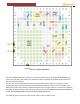
Figure 6-2: Antenna Pad Ground Cutout (Top View)
For routing microstrip lines UNDERNEATH the NAD on layer 1, these ground cutouts internal to the
NAD need to be accounted for in the stripline calculation. The internal GND height and dielectric constant
of the NAD board are shown below:
H = 19.3 mils (491 micron)
Dielectric Constant = 4.1
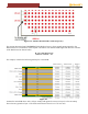
For example, consider the following stackup for a main PCB:
Figure 6-3
Assume the main PCB above with a 6 layer stackup with ground cut away on layer 2 so the microstrip
lines reference ground on layer 3. The dielectric thickness from L1 to L3 is 21.2 mils.