
User's Guide


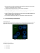


Figure 5: Microstrip Impedance Calculations
Due to the nature of the weave chosen for each PCB, the dielectric constant of the NAD board is 4.1 while
the main board is 4.3. A dielectric constant of 4.2 was chosen in the stripline calculation, while 4.3 was
used for the microstrip calculation.
Main board stack up may vary so these line widths may need to be recalculated. IT IS HIGHLY
RECOMMENDED TO USE A SIMILAR STACKUP AS SHOWN IN FIGURE 3.
Antenna Routing Recommendations:
1. Microstrip routes on layer1 and very short route under the NAD.
Figure 6: Antenna Line Microstrip Routes on Layer1
2. Then routes to inner layer and continues route as stripline.