
Product Info

LT103OEM UWB Radar Module
Rev.2.1 Pag. 8 of 14
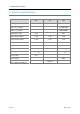
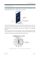
6 Pin-out description
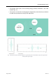
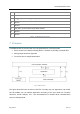
The LT103OEM pin-out reference drawing and functionality is described in Fig. 2 and Table
2 respectively.
Fig. 5: Reference Drawing for Pin Out (top-side, top-view)
Pin
Description
1
Ground
2
CKIO_P <In/Out> LVDS Synchronization Clock Pos (multi-module)
3
CKIO_N<In/Out> LVDS Synchronization Clock Neg (multi-module)
4
Ground
5
Vdd
RF
: RF Power Supply Voltage (may be shorted to P19)
6
Ground
7
Ground
8
SYSRST: system reset (active low)
9
SWDCLK: Debugger Clock
10
SWDIO: Debugger I/O
11
Ground
12
Ground
13
Ground
14
Ground
15
Ground
16
UART_RX: UART Receiver Pin