Revision 1.1 as of 2013-11-13 Firmware 0 (build 3795), Driver v0.9.22 cronologic GmbH & Co.
Contents 1 Introduction 1.1 Features . . . . . . . . . . . . . . . . . . . . . . . . . . . . . . . . . . . . . . . . . 1 1 2 Hardware 2.1 Installing the Board . . . . . . . . . . . . . . 2.2 External Inputs and Connectors . . . . . . . . 2.2.1 Connectors . . . . . . . . . . . . . . . 2.2.2 Analog Inputs . . . . . . . . . . . . . 2.2.3 Digital Inputs . . . . . . . . . . . . . . 2.3 Extension Card . . . . . . . . . . . . . . . . . 2.4 Ndigo250M-14 Functionality . . . . . . . . . . 2.4.1 Zero Suppression .
Contents 3.4 . . . . . . . . . . . . 32 32 34 35 36 37 38 39 39 39 41 41 4 Packet Format 4.0.2 Output Structure ndigo packet . . . . . . . . . . . . . . . . . . . . . . . . 43 43 5 C Example 45 6 Technical Data 6.1 Operating Conditions . . . . . . . . . . . . . . 6.1.1 Environmental Conditions for Operation 6.1.2 Environmental Conditions for Storage . 6.2 Digitizer Characteristics . . . . . . . . . . . . . 6.3 TDC Characteristics . . . . . . . . . . . . . . . 6.4 Electrical Characteristics . . . . .
1 Introduction The Ndigo250M and Ndigo125M are digitizer and transient recorders designed to sample relatively shorts pulses in rapid repetition. They produce a stream of output packets, each containing data from a single trigger event together with a timestamp. 1.
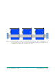
2 Hardware 2.1 Installing the Board The Ndigo250M-14 board can be installed in any PCIe slot with eight or more lanes. If the slot electrically supports less than 8 lanes, the board will operate at lower data throughput rates. Using a single Ndigo250M, no further connections need to be made. For applications that require more than four ADC channels, several Ndigo boards can be operated in sync.
termination C2 C2 C2 termination C1 C1 C1 Figure 2.1: If several Ndigo boards are connected to work in sync , the boards must be connected using a ribbon cable as bus for synchronization and trigger signals. Proper termination is required at both ends of the cable. cronologic GmbH & Co.
2.2 External Inputs and Connectors 2.2.1 Connectors Trigger T Gate D C B A G Ndigo 250M-14 cronologic The inputs of the Ndigo250M-14 are located on the PCI bracket. Figure 2.3 on page 5 shows the location of the 4 analog inputs A to D and the two digital inputs G (GATE) and T (TRIGGER). Furthermore, a board interconnection connector (C2) can be found at the top edge of the Ndigo250M-14, as displayed in Figure 2.3 on page 5. Connector C2 is used as a bus interface between multiple Ndigo boards.
450MHz offset + - Figure 2.4: Input circuit for each of the four analog channels. 2.2.2 Analog Inputs The analog inputs of the ADC are single ended LEMO00 coax connectors. The inputs have a 50Ω impedance and are DC coupled. The inputs are converted to a differential signal using an operational amplifier. The input voltage range is 1Vp-p centered around a programmable offset voltage. See section 6.4.3 for details. Analog Offsets +0.5V +0.5 V 0.2V -0.5 V -0.
6.4.3. This feature is especially useful for highly asymmetric signals, such as pulses from TOF +0.5V +0.5V 0.43V -0.5 V -0.5 V analog_offset[i] = 0V analog_offset[i] = -0.43V Figure 2.6: Asymmetric signal shifted to increase dynamic range spectrometers or LIDAR systems. By shifting the DC baseline to one end of the ADC range, the input range can be used fully, providing the maximum dynamic range. 2.2.3 Digital Inputs There are two digital inputs on the front slot cover called TRIGGER and GATE.
1,0V analog_offset[4] -1,0V Figure 2.8: For TRIGGER and GATE negative thresholds can be set to support negative signals such as 16mA NIM. TDC on Input TRIGGER There is a TDC connected to the input TRIGGER. When used with the TDC, input TRIGGER supports negative pulses only and analog offset[4] must be negative. The TDC creates packets of type 8. These packets first contain a coarse timestamp and a payload that can be used to calculate the trigger position with higher precision.
2.4 Ndigo250M-14 Functionality The analog input signal is quantized to 14 bits. However, the board always scales and offsets the data to 16 bit signed data centered around 0. Interleaving of multiple channels is not supported 2.4.1 Zero Suppression One of Ndigo250M’s key features is on-board zero suppression to reduce PCIe bus load. Only data that passes specifications predefined by the user is transmitted. This guide refers to the data structure in which wave form data is transmitted as “packets”.
2.4.2 Trigger Blocks The Ndigo250M-14 records analog wave forms using zero suppression. Whenever a relevant waveform is detected, data is written to an internal FIFO memory. Each ADC channel has one trigger block determining whether data is written to the FIFO. The parameters are set in Structure ndigo trigger block(See chapter 3.4.3 on page 35). Each trigger block consists of two independent units that check the incoming raw data stream for trigger conditions (Fig. 2.9 on page 9).
total length = 19 length = 12 threshold precursor = 6 Figure 2.10: Parameters for edge triggering total length = 21 length = 6 threshold precursor = 6 Figure 2.11: Parameters for level triggering cronologic GmbH & Co.
trigger 1 Z-1 sample data threshold rising edge trigger 2 Z-1 threshold rising edge Figure 2.12: From the ADC inputs, a trigger unit creates an input flag for the trigger matrix. Each digitizer channel (A, B, C, D) has two trigger units. Z-1 input rising edge Figure 2.13: The digital inputs TRIGGER, GATE, BUS0, BUS1, BUS2 and BUS3 have trigger units without a programmable threshold. cronologic GmbH & Co.
ext0 extension sync0 block ext1 extension sync1 block ext2 extension sync2 block ext3 extension sync3 block digital trigger digital trigger digital trigger digital trigger digital trigger bus0_pe bus0 bus1_pe bus1 bus2_pe bus2 bus3_pe bus3 1 func_trig GATE gate_pe gate TRIGGER D1 digital trigger tdc_pe tdc analog trigger C0 C1 D analog trigger D0 C B0 B1 B analog trigger A1 analog trigger A0 A Gates trigger_ block[0] trigger_ block[1] trigger_ block[2] trigger_ block[3] time st
2.4.3 Gating Blocks Figure 2.15: Gating Blocks: Each gating block can use an arbitrary combination of inputs to trigger its state machine. The outputs can be individually inverted and routed to the AND-gate feeding the trigger blocks. To decrease the amount of data transmitted to the PC, the Ndigo250M-14 includes 4 independent gate and delay units. A gate and delay unit creates a gate window starting at a specified time after a trigger, closing the window at gate stop.
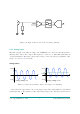
Figure 2.16 shows the functionality of the gate timing and delay unit. Active gate time is marked in green. Trigger Gate Gate Start Gate Stop Figure 2.16: Gate and delay functionality: When a trigger occurs, the gate opens after a set period of time (“gate start”) and closes when it reaches “gate stop”.
its output after the specified delay. To send this pulse to the trigger block, the gating block must be enabled in the trigger block’s AND matrix and the ONE trigger source must be selected. 2.4.4 Auto Triggering Function Generator Some applications require periodic or random triggering. Ndigo250M’s function generator provides this functionality. The delay between two trigger pulses of this trigger generator is the sum of two components: A fixed value M and a pseudo random value given by the exponent N.
2.5 Multiple Ndigo boards synchronization Using several Ndigo devices in applications that use more channels than a single board can provide requires synchronized operation. To ensure exact synchronization, a delay parameter needs to be set for each board. This parameter might change in case boards are swapped, added or removed and in some cases might change after a firmware update. The calibration tool “MultiboardCalibration.exe” is available after installing the Ndigo device driver.
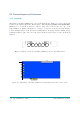
2.5.1 Calibration Procedure 1. Make sure the “Automode” is selected. 2. Record the calibration histograms by pressing “Record histograms”. The program will perform up to 200 measurements of the sync delay. After accumulating some data, the delay values found are reported in the column “AutoMmt”. The values can be verified by examining histogram that was recorded. A board’s histogram should look like the one shown in Figure 2.18.
Figure 2.18: Histogram for the case the delay value for the board is not set correctly. Please note: the lower panel might differ from board to board, with the “step” being at a different position. Figure 2.19: Histogram for the case the delay value for the board is set correctly. Please note: the lower panel might differ from board to board, with the “step” being at a different position. cronologic GmbH & Co.
2.5.2 Synchronizing with an HPTDC8-PCI The Ndigo250M-14 does not support synchronization with an HPTDC8-PCI. cronologic GmbH & Co.
2.6 Performing a firmware update After installing the Ndigo device driver, a firmware update tool is available. By choosing “NdigoFirmwareGUI.exe” a firmware update can be performed. After invoking the application a window as shown in Figure 2.20 will appear. The tool can be used for updating the firmware and to create a backup of the on-board calibration data of the Ndigo unit. If several boards are present, the one which is going to be used can be selected in the upper left corner of the window.
information shown in the upper half of the application window does not change right after flashing a new firmware. 2.6.1 Calibrating the TDC After each update of the Ndigo250M-14 firmware the TDC has to be calibrated. The calibration is done with the tool “TDC Calibration.exe” which is available after installing the Ndigo device driver. After invoking the application a window as shown in Figure 2.21 will appear. Figure 2.21: The TDC calibration tool as provided with the Ndigo device driver.
tion data on the card. 6. Calibration done! The card can only be successfully calibrated if: First Bin is in the range of 4 to 16 Empty Bins is less than (First Bin + 4) at least 10,000 events have been captured a valid serial number is set. Important note: If the application reports an error check if the input pulse is within specification. cronologic GmbH & Co.
cronologic GmbH & Co.
3 Driver Programming API The API is a DLL with C linkage. There also exists a .Net wrapper. The functions provided by the DLL are declared in Ndigo250M interface.h and Ndigo common interface.h. 3.1 Constants #define NDIGO250M CHANNEL COUNT 4 The number of analog input channels. #define NDIGO250M GATE COUNT 4 The number of gating blocks. #define NDIGO250M TDC COUNT 1 The number of TDC channels. #define NDIGO250M DMA COUNT 6 The number of DMA channels.
3.2 Initialization int ndigo250m count devices(int *error code, char **error message) Return the number of boards that are supported by this driver in the system. int ndigo250m get default init parameters(ndigo init parameters *init) Get a set of default parameters to feed into ndigo init(). This must always be used to initialize the ndigo init parameter structure.
ndigo bool t is slave Data acquisition of this board is controlled by the master board. int sync period Period of the multicard sync pulse. Ignored for single board setups. Should be set to 4 if only Ndigo5G and Ndigo250M boards are present in the system. If other boards are synchronized the correct value is the lowest common denominator of the value of all boards. int sync delay Fine tap delay for incoming sync signals. Ignored for single board setups. int sync delay master Fine tap delay for sync signals.
3.3 Status Information 3.3.1 Functions for Information Retrieval The driver provides functions to retrieve detailed information on the type of board, its configuration, settings and state. The information is split according to its scope and the computational requirements to query the information from the board. int ndigo get static info(ndigo device *device,ndigo static info *info) This structure contains information about the board that does not change during run time.
A change in the first digit generally requires a recompilation of user applications. Change in the second digit denote significant improvements or changes that don’t break compatibility and the third digit changes with minor bugfixes and similar updates. int firmware revision Firmware revision of the FPGA configuration. This increments only when there is a functional change. int board revision int board configuration Describes the schematic configuration of the board.
3.3.3 Structure ndigo param info int size The number of bytes occupied by the structure. int version A version number that is increased when the definition of the structure is changed. The increment can be larger than one to match driver version numbers or similar. double bandwidth Analog Bandwidth setting of the ADC. Should be 450MHz. double sample rate Sample rate currenly used. sample rate = 2.5e8/divisor. double sample period The period one sample in the data represents in picoseconds.
Alert flags from the system monitor and temperature sensor. Bits 0 to 3 are measured by the system monitor of the FPGA. Bits 4 and 5 are provided by an external temperature sensor. Bit Bit Bit Bit Bit Bit 0 1 2 3 4 5 : : : : : : FPGA temperature alert (> 85◦ C) Internal FPGA voltage out of range (< 1.01V or > 1.08V ) FPGA auxiliary voltage out of range. (< 2.375V or > 2.
3.4 Configuration The device is configured with a configuration structure. The user should first obtain a structure that contains the default settings of the device read from an on board ROM , than modify the structure as needed for the user application and use the result to configure the device.
Configuration of the external trigger sources. Threshold is ignored for entries 8 and above.
T = 1 + M + [1...2N ] (3.1) 0 ≤ M < 232 (3.2) 0 ≤ N < 32 (3.3) clock cycles. There is no enable or reset as the usage of this trigger can be configured in the trigger block channel source field. int divisor The 500MHz base clock is divided by this divisor to create the rsampling frequency. Valid values are 2 to 32 for the Ndigo250M and 4 to 32 for the Ndigo125M. int high gain[2] If set to 1 the input gain is boosted by 3.5dB. Gain[0] modifies channels 0 and 1, gain[1] modifies channels 2 and 3.
For trigger indices NDIGO TRIGGER AUTO and NDIGO TRIGGER ONE this is ignored. For trigger indices NDIGO TRIGGER TDC PE to NDIGO TRIGGER BUS3 PE this must be set. 3.4.3 Structure ndigo trigger block ndigo bool t enabled Activate triggers on this channel. ndigo bool t retrigger If a new trigger condition occurs while the postcursor is acquired the packet is extended by starting a new postcursor. Otherwise the new trigger is ignored and the packet ends after the precursor of the first trigger.
#define #define #define #define #define #define #define #define #define #define #define #define #define NDIGO NDIGO NDIGO NDIGO NDIGO NDIGO NDIGO NDIGO NDIGO NDIGO NDIGO NDIGO NDIGO TRIGGER TRIGGER TRIGGER TRIGGER TRIGGER TRIGGER TRIGGER TRIGGER TRIGGER TRIGGER TRIGGER TRIGGER TRIGGER SOURCE SOURCE SOURCE SOURCE SOURCE SOURCE SOURCE SOURCE SOURCE SOURCE SOURCE SOURCE SOURCE GATE BUS0 BUS1 BUS2 BUS3 AUTO ONE TDC PE GATE PE BUS0 PE BUS1 PE BUS2 PE BUS3 PE 0x00000200 0x00000400 0x00000800 0x00001000 0x000
created. NOT IMPLEMENTED ndigo bool t reserved1 Defaults to false. Do not change. int start The number of samples from the first input signal seen in the idle state until the gating output is set. int stop The number of samples from leaving the idle state until the gating output is reset. If retriggering is enabled the timer is reset to the value of the start parameter whenever the input signal is set while waiting to reach the stop time.
3.4.6 Run Time Control int ndigo start capture(ndigo device *device) int ndigo pause capture(ndigo device *device) int ndigo continue capture(ndigo device *device) Call this to resume data acquisition after a call to ndigo pause capture. int ndigo stop capture(ndigo device *device, int channel mask) int ndigo single shot(ndigo device *device, int channel mask) Enable the selected channels. A channel is disabled again immediately after the first trigger on that channel.
3.5 Readout int ndigo250m read(ndigo device *device, ndigo250m read in *in, ndigo250m read out *out) For each DMA channel returns a pointer to an array of captured data in read out. The result can contain any number of packets of type ndigo packet. read in provides parameters to the driver. A call to this method automatically allows the driver to reuse the memory returned in the previous call. Returns an error code as defined in the structure ndigo read out.
separately for each channel. cronologic GmbH & Co.
3.6 Other Functions 3.6.1 LED control There are six LEDs on the front panel. The intensity of the red and green part can be set from 0 to 255. There is no blue component in the current version. Per default all LEDs are set to auto mode. This means that used channels are lit green, activity is shown as yellow on overflow is shown as red. int ndigo set led color(ndigo device *device, int led, unsigned short r, unsigned short g, unsigned short b) Set the LED to the selected color.
cronologic GmbH & Co.
4 Packet Format 4.0.2 Output Structure ndigo packet unsigned char channel 0 to 3 for the ADC input channels, 4 for the TDC, 5 for the timestamp channel. unsigned char card Identifies the source card in case there are multiple boards present. Defaults to 0 if no value is assigned to the parameter board id in Structure ndigo init parameters or set via int ndigo set board id(ndigo device *device, int board id). unsigned char type For the ADC channels this is set to 1 to signify 16 bit signed data.
Number of 64-bit elements (each containing 4 samples) in the data array if type < 128. If type = 128 this is the pattern of trigger sources that where active in the clock cycle given by the timestamp. Bits are set according to the trigger sources, i.e. bit 0 is set if trigger A0 was active, bit 29 is set if trigger BUS3 PE was active. Use the NDIGO TRIGGER SOURCE * # defines to check for the bits set. unsigned int64 timestamp ADC channels A to D: Timestamp of the last word in the packet in ps.
5 C Example 1 #i n c l u d e ” N d i g o i n t e r f a c e . h” 2 #i n c l u d e 3 #i n c l u d e < s t d l i b . h> 4 5 i n t main ( i n t a r g c , char * a r g v [ ] ) 6 { 7 n d i g o i n i t p a r a m e t e r s params ; 8 n d i g o g e t d e f a u l t i n i t p a r a m e t e r s (¶ms ) ; 9 10 params . c a r d i n d e x = 0 ; 11 params . b u f f e r s i z e [ 0 ] = 1<<23; 12 params . d r i v e e x t e r n a l c l o c k = t r u e ; 13 params . i s s l a v e = f a l s e ; 14 params .
39 40 41 42 43 44 45 46 47 48 49 50 51 52 53 54 55 56 57 58 59 60 61 62 63 64 65 66 67 68 69 70 71 72 73 74 75 76 77 78 79 80 81 82 83 84 c o n f i g . t r i g g e r b l o c k [ 0 ] . s o u r c e s = NDIGO TRIGGER SOURCE A0 ; config . t r i g g e r b l o c k [ 0 ] . length = 16; c o n f i g . t r i g g e r b l o c k [ 0 ] . g a t e s = NDIGO TRIGGER GATE NONE ; config . analog offset [0] = 0.1; c o n f i g . t r i g g e r [ NDIGO TRIGGER A0 ] . edge = t r u e ; c o n f i g .
85 86 87 88 89 90 91 92 packet = next packet ; c o u n t ++; } } } n d i g o c l o s e ( ndgo ) ; return0 ; } cronologic GmbH & Co.
cronologic GmbH & Co.
6 Technical Data 6.1 Operating Conditions 6.1.1 Environmental Conditions for Operation The board is designed to be operated under the following conditions: Symbol Parameter ambient temperature relative humidity at 31◦ C Min 5 20 Typ Max 40 75 Units ◦ C % 6.1.2 Environmental Conditions for Storage The board shall be stored between operation under the following conditions: Symbol Parameter ambient temperature relative humidity at 31◦ C non condensing Min -30 10 Typ Max 60 70 Units ◦ C % 6.
6.3 TDC Characteristics Symbol BINTDC INLTDC Parameter TDC bin size TDC integral nonlinearity Input Pulse Width Input Pulse Spacing (Deadtime) Min Typ Max 3.3 32 Units ps ns ns 6.4 Electrical Characteristics 6.4.1 Oscillator The Ndigo250M-14 uses an OCXO oscillator with 25ppb stability. After power up the oscillator needs to run for 10 minutes to reach this stability 6.4.
Symbol VDth Vdn Vdn ZD Parameter discrimination threshold recommended amplitude for negative pulses recommended amplitude for negative pulses input impedance cronologic GmbH & Co. KG 51 Min -1.25 -0.1 - VDth 0.1 + VDth Typ 2VDth 2VDth 50 Max 1.25 1.25 - VDth 1.
6.5 Information Required by DIN EN 61010-1 6.5.1 Manufacturer The Ndigo250M-14 is a product of: cronologic GmbH & Co. KG Jahnstraße 49 60318 Frankfurt HRA 42869 beim Amtsgericht Frankfurt/M VAT-ID: DE235184378 6.5.2 Intended Use and System Integration The devices are not ready to use as delivered by cronologic. It requires the development of specialized software to fulfill the application of the end user.
6.5.4 Environmental Conditions Refer to the sections on Environmenal Conditions on page 49 6.5.5 Inputs The analog inputs are DC coupled. The inputs have very high input bandwidth requirements and therefore there are no circuits that provide over voltage protection for these signals. Any voltage on the inputs above 5V or below -3V relative to the voltage of the slot cover can result in permanent damage to the board. 6.5.