Revision 0.2.31 as of 2014-10-28 Firmware 2 (build 4739), Driver v0.9.39 cronologic GmbH & Co.
Contents 1 Introduction 1.1 Features . . . . . . . . . . . . . . . . . . . . . . . . . . . . . . . . . . . . . . . . . 1 1 2 Hardware 2.1 Installing the Board . . . . . . . . . . . . . . . . . . . . 2.2 Ndigo5G External Inputs and Connectors . . . . . . . . 2.2.1 Connectors . . . . . . . . . . . . . . . . . . . . . 2.2.2 Analog Inputs . . . . . . . . . . . . . . . . . . . 2.2.3 Digital Inputs . . . . . . . . . . . . . . . . . . . . 2.3 Extension Card . . . . . . . . . . . . . . . . . . . . . . . 2.
Contents 3.5 . . . . . 38 38 38 38 38 4 Packet Format 4.0.2 Output Structure ndigo packet . . . . . . . . . . . . . . . . . . . . . . . . 41 41 5 C Example 43 6 Technical Data 6.1 Digitizer Characteristics . . . . . . . . . . . . . 6.1.1 1-Channel-Mode (5Gsps) . . . . . . . . 6.1.2 2-Channel-Mode (2.5 Gsps) . . . . . . . 6.1.3 4-Channel-Mode (1.25 Gsps) . . . . . . 6.2 Electrical Characteristics . . . . . . . . . . . . 6.2.1 Oscillator . . . . . . . . . . . . . . . . . 6.2.
1 Introduction The Ndigo5G is a digitizer and transient recorder designed to sample relatively shorts pulses in rapid repetition. It produces a stream of output packets, each containing data from a single trigger event together with a timestamp. 1.1 Features 10 bit dynamic range up to 5 Gsps sample rate (in 1 channel mode) up to 4 channels digital input with TDC that can also be used for gating and triggering 2nd digital input for gating or triggering PCIe 4x 1.
2 Hardware 2.1 Installing the Board The Ndigo5G board can be installed in any x4 (or higher amount of lanes) PCIe slot. If the slot electrically supports less than 4 lanes, the board will operate at lowerdata throughput rates. Please ensure proper cooling of the device. The Ndigo5G has an onboard temperature detection. If the ADC chip temperature exceeds 90◦ C a warning is issued to the device driver. In case the temperature is higher than 95◦ C the ADC is disabled to avoid damage.
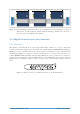
termination C2 C2 C2 termination C1 C1 C1 Figure 2.1: If several Ndigo boards are connected to work in sync , the boards must be connected using a ribbon cable as bus for synchronization and trigger signals. At both ends of the cable, proper termination is required. 2.2 Ndigo5G External Inputs and Connectors 2.2.1 Connectors The inputs of the Ndigo5G are located on the PCI bracket. Figure 2.
C2 C1 T D C B A G Figure 2.3: Schematics of an Ndigo5G board showing inter-board connectors C1 and C2. 2.2.2 Analog Inputs LemoD00 connector EV10AQ190 DAC TC1-1-I3M+ analog-offset[i] Figure 2.4: Input circuit for each of the four analog channels. The analog inputs of the ADC are single ended LEMO00 coax connectors. The inputs have a 50Ω impedance and are AC coupled. The inputs are converted to a differential signal using a balun.
+0,25V +0,25V 0,1V -0,25V -0,25V analog_offset[i] = 0V analog_offset[i] = 0,1V Figure 2.5: Users can add analog offset to the input before sampling +0,25V +0,25V 0,22V -0,25V -0,25V analog_offset[i] = 0V analog_offset[i] = -0,22V Figure 2.6: Asymmetric signal shifted to increase dynamic range 2.2.3 Digital Inputs There are two digital inputs on the front slot cover called Trigger and GATE. Both inputs provide a digital input signal routed to the trigger matrix.
2.3 Extension Card The Ndigo Extension card provides additional inputs or outputs to the FPGA. It is connected to the Samtec QSS-025 connector on an Ndigo5G by an Samtec SQCD cable assembly. The Ndigo Extension Card provides up to ten single ended LEMO00 connectors. The circuit connecting to each of these circuits can be chosen to provide inputs or outputs. These can be AC or DC coupled. AC coupled inputs support NIM signaling. The signals connect to 2.5V IO Pins of the Xilinx Virtex-5 FPGA.
2.4.1 ADC Modes Depending on board configuration, the analog input signal is quantized to 8 or 10 bits. However, the board always scales and offsets the data to 16 bit signed data centered around 0. Data processing such as trigger detection or packet building are always performed on 3.2ns intervals. Depending on the ADC mode, this interval may contain 4, 8 or 16 samples. The board supports using one, two or four channels: 1 Channel Modes A, B, C and D In these modes, only a single channel is used.
1.25 GHz CLK (2.5 GHz) Clock circuit ADC A 1.25 Gsps ADC B 1.25 Gsps ADC C 1.25 Gsps ADC D 1.25 Gsps AAI, AAIN BAI, BAIN CAI, CAIN DAI , DAIN Figure 2.7: ADCs in 4 channel mode ABCD at 1.25Gsps. Inverted 1.25 GHz CLK (2.5 GHz) Clock, circuit ADC,A 1.25 Gsps ADC,B 1.25 Gsps ADC,C 1.25 Gsps ADC,D 1.25 Gsps In-phase 1.25 GHz AAI,,AAIN DAI,,DAIN Figure 2.8: ADCs in 2 channel mode AD, interleaved for 2.5Gsps. 90 0 phase-shifted 2700 phase -shifted 1.25 GHz 1.25 GHz CLK 72.
2.4.2 Zero Suppression One of Ndigo 5G’s key features is on-board zero suppression to reduce PCIe bus load. Only data that passes specifications predefined by the user is transmitted. This guide refers to transmitted wave form data as “packets”. A packet contains the wave form data and a timestamp giving the absolute time (i.e. the time since start of data acquisition) of the packet’s last sample. Figure 2.10 shows a simple example: Data is written to the PC only if values exceed a specified threshold.
precursor + length + 1 cycles of 3.2ns. For level triggering, packet length is data dependent (Figure 2.12 on page 12). Please note that triggering is not accurate to sample. For each 3.2ns clock cycle, it is determined whether on any sample during that clock cycle a trigger condition is met. The clock cycle is then selected as the trigger point. As a result, the trigger sample can be anywhere within a range of up to 16 samples in single channel mode (Figure 2.15 on page 13) at 16 samples per 3.2ns.
total length = 21 length = 6 threshold precursor = 6 Figure 2.12: Parameters for level triggering total length = 4 precursor = 1 threshold length = 2 3200 ps Figure 2.13: Triggering in 4 channel mode at 4 samples per clock cycle. total length = 4 precursor = 1 threshold length = 2 3200 ps Figure 2.14: Triggering in 2 channel mode at 8 samples per clock cycle. cronologic GmbH & Co.
total length = 4 precursor = 1 threshold length = 2 3200 ps Figure 2.15: Triggering in 1 channel mode at 16 samples per clock cycle. trigger 1 Z-1 sample data threshold rising edge trigger 2 Z-1 threshold rising edge Figure 2.16: From the ADC inputs, a trigger unit creates an input flag for the trigger matrix. Each digitizer channel (A, B, C, D) has two trigger units. Z-1 input rising edge Figure 2.17: The digital inputs Trigger, GATE, BUS0, BUS1, BUS2 and BUS3 have simpler trigger units.
enable extension input ignore_cable cable sync Figure 2.18: The extension block combines signals from the optional extension board and the sync cable.
2.4.4 Gating Blocks Trigger Figure 2.20: Gating Blocks: Each gating block can use an arbitrary combination of inputs to trigger its state machine. The outputs can be individually inverted and routed to the AND-gate feeding the trigger blocks. To decrease the amount of data transmitted to the PC, Ndigo5G includes 4 independent gate and delay units. A gate and delay unit creates a gate window starting at a specified time after a trigger, closing the window at gate stop.
Trigger Gate Gate Start Gate Stop Figure 2.21: Gate and delay functionality: When a trigger occurs, the gate opens after a set period of time (“gate start”) and closes when it reaches “gate stop”. Gating Example 1: Suppression of Noise After Starting an Acquisition In mass spectrometer and other experiments, noise while starting data acquisition can result in undesired trigger events for that time period.
Since the triggers are only connected by OR in the triggerblock logic (see fig. 2.19) they are assigned to one of the gates each and connected with AND via the gating block region of the trigger matrix (see fig. 2.19 and 2.23). Because of the dead times of the gates it is important to enable the retriggering feature. Furthermore a precursor of 2 clock cycles is needed, because the gates are delayed in relation to the ADC samples.
Trigger Figure 2.23: Gating block logic for the AND connection of two triggers. 2.4.5 Auto Triggering Function Generator Some applications require periodic or random triggering. Ndigo5G’s function generator provides this functionality. The delay between two trigger pulses of this trigger generator is the sum of two components: A fixed value M and a pseudo random value given by the exponent N. The period is T = 1 + M + [1...2N ] (2.1) clock cycles with a duration of 3.2 ns per cycle.
time of the trigger event except for the period monitor. Only one packet is created, no matter how many trigger sources caused the timestamp channel to trigger. 2.4.7 Data Lookup Table In some applications it might be useful to modify the ADC sample data by a user defined function f (x). In this case the onboard FPGA is able to perform this task such that the the data stream consists of data words f (sample) instead of sample.
Flashing the values might take up to 10 seconds during which the program might not respond. Important note:If the application reports a “PLL not locked” error check the cable. If the recording of histograms does not make progress check the cable. Make sure the cable is properly terminated at both ends and firmly attached to each card. 2.5.1 Calibration Procedure 1. Make sure the “Automode” is selected. 2. Record the calibration histograms by pressing “Record histograms”.
Figure 2.25: Histogram for the case the delay value for the board is not set correctly. Please note: the lower panel might differ from board to board, with the “step” being at a different position. Figure 2.26: Histogram for the case the delay value for the board is set correctly. Please note: the lower panel might differ from board to board, with the “step” being at a different position. cronologic GmbH & Co.
2.5.2 Synchronizing a Ndgio5G and an HPTDC8-PCI In order to operate a Ndigo5G in sync with one ore more HPTDC8-PCI boards, a board to board in -terconnection using a Ndigo Extension Board needs to be done. The Ndigo Extension Board has four clock outputs. One of them needs to be connected to the external clock input of the HPTDC using a standard Lemo 00 cable. The Ndigo5G is connected to the Ndigo Extension Board using the Samtec ribbon cable provided with the Ndigo Extension Board.
Figure 2.28: The firmware update and calibration data backup tool as provided with the Ndigo device driver. information shown in the upper half of the application window does not change right after flashing a new firmware. After flashing and shutting the PC or the crate off and on again it is recommended to perform a window calibration. The tool “WindowCalibration” is provided for that purpose within the driver installation.
Figure 2.29: The TDC calibration tool as provided with the Ndigo device driver. tion data on the card. 6. Calibration done! The card can only be successfully calibrated if: First Bin is in the range of 4 to 16 Empty Bins is less than (First Bin + 4) at least 10,000 events have been captured a valid serial number is set. Important note: If the application reports an error check if the input pulse is within specification. cronologic GmbH & Co.
3 Driver Programming API The API is a DLL with C linkage. There exists also a .Net wrapper. The functions provided by the DLL are declared in Ndigo interface.h. 3.1 Constants #define NDIGO CHANNEL COUNT 4 The number of analog input channels. #define NDIGO GATE COUNT 4 The number of gating blocks. #define NDIGO TRIGGER COUNT 16 The number of triggers. Two per analog input, one per digital input plus some specials. #define NDIGO ADD TRIGGER COUNT 6 Additional set of triggers for digital inputs. 3.
int card index The index in the list of Ndigo5G boards that should be initialized. There might be multiple boards in the system that are handled by this driver as reported by ndigo count devices. This index selects one of them. Boards are enumerated depending on the PCIe slot. The lower the bus number and the lower the slot number the lower the card index. int board id This 8 bit number is filled into each packet created by the board and is useful if data streams of multiple boards will be merged.
#define CRONO DEVICE NDIGO250M 2 3.3 Status Information 3.3.1 Functions for Information Retrieval The driver provides functions to retrieve detailed information on the type of board, its configuration, settings and state. The information is split according to its scope and the computational requirements to query the information from the board. int ndigo get static info(ndigo device *device,ndigo static info *info) This structure contains information about the board that does not change during run time.
int board revision 0 for experimental prototypes labeled “Rev. 1” 2 for the version produced until 2010 labeled “Rev. 2”‘ 3 for the version produced starting in 2011 labeled “Rev. 3” int board configuration Describes the schematic configuration of the board. For board revision 0 this always reads 0. For board revision 2 the following assignments are valid: If Bit 3 = 0 this following is valid: Bit 0 determines the ADC resolution. (0 = 8 − bit or 1 = 10 − bit ).
If not 0 the driver found valid calibration data in the flash on the board and is using it. ndigo bool t dc coupled Returns false for the standard AC coupled Ndigo5G. int subversion revision A number to track builds of the firmware in more detail than the firmware revision. It changes with every change in the firmware, even if there is no visible effect for the user. char calibration date[20] DIN EN ISO 8601 string YYYY-MM-DD HH:DD describing the time when the card was calibrated. 3.3.
int adc rpm Speed of the ADC fan. Reports 0 if no fan is present. int fpga rpm Speed of the FPGA fan. Reports 0 if no fan is present. int alerts Alert bits from the system monitor. Bit Bit Bit Bit Bit Bit 0 1 2 3 4 5 : : : : : : FPGA temperature alert (> 85◦ C) Internal FPGA voltage out of range (< 1.01V or > 1.08V ) FPGA auxiliary voltage out of range. (< 2.375V or > 2.
int ndigo get current configuration(ndigo device *device, ndigo configuration *config) int ndigo configure(ndigo device *device, ndigo configuration *config) int ndigo set board id(ndigo device *device, int board id) The board id can be changed after initialization of the card. If cronotools are used the board id changes have to be done before cronotools initialization. 3.4.1 Structure ndigo configuration This is the structure containing the configuration information.
ndigo bool t tdc enabled Enable capturing of TDC measurements on external digital input channel. ndigo bool t tdc fb enabled Enable enhanced TDC resolution. Currently not implemented. double analog offset[NDIGO CHANNEL COUNT] Sets the input DC offset-values to +- this value in volts. Defaults to 0. double dc offset[2] Sets the DC offset in volts for the TDC trigger input (index 1) and the GATE input (index 0). The trigger threshold is zero. For negative 0.8V NIM pulses a value of 0.4 should be set here.
Enable output drive for each of the four external sync lines. Each integer represents a bitmask selecting the trigger sources for that line. The bit mapping is described in section “Structure ndigo trigger block” on page 34. int auto trigger period int auto trigger random exponent Create a trigger either periodically or randomly. There are two parameters M = trigger period and N = random exponent that result in a distance between triggers of T = 1 + M + [1...2N ] (3.1) 0 ≤ M < 232 (3.2) 0 ≤ N < 32 (3.
For trigger indices NDIGO TRIGGER TDC to NDIGO TRIGGER BUS3 PE the threshold is ignored. ndigo bool t edge If set this trigger implements edge trigger functionality else this is a level trigger. For trigger indices NDIGO TRIGGER AUTO and NDIGO TRIGGER ONE this is ignored. For trigger indices NDIGO TRIGGER TDC PE to NDIGO TRIGGER BUS3 PE this must be set. ndigo bool t rising If set trigger on rising edges or when above threshold. For trigger indices NDIGO TRIGGER AUTO and NDIGO TRIGGER ONE this is ignored.
#define NDIGO TRIGGER SOURCE A0 0x00000001 #define NDIGO TRIGGER SOURCE A1 0x00000002 #define NDIGO TRIGGER SOURCE B0 0x00000004 #define NDIGO TRIGGER SOURCE B1 0x00000008 #define NDIGO TRIGGER SOURCE C0 0x00000010 #define NDIGO TRIGGER SOURCE C1 0x00000020 #define NDIGO TRIGGER SOURCE D0 0x00000040 #define NDIGO TRIGGER SOURCE D1 0x00000080 #define NDIGO TRIGGER SOURCE TDC 0x00000100 #define NDIGO TRIGGER SOURCE GATE 0x00000200 #define NDIGO TRIGGER SOURCE BUS0 0x00000400 #define NDIG
space only in case the FIFO is full. Therefore, if this number is 1.0 or more at least every second packet in the DMA buffer is guaranteed to have the full length set by the gatelength parameters. In many cases smaller values will also result in full length packets. But below a certain value multiple packets that are cut off at the end will show up. 3.4.4 Structure ndigo gating block ndigo bool t negate Invert output polarity. Defaults to false. ndigo bool t retrigger Defaults to false.
#define NDIGO TRIGGER SOURCE A0 0x00000001 #define NDIGO TRIGGER SOURCE A1 0x00000002 #define NDIGO TRIGGER SOURCE B0 0x00000004 #define NDIGO TRIGGER SOURCE B1 0x00000008 #define NDIGO TRIGGER SOURCE C0 0x00000010 #define NDIGO TRIGGER SOURCE C1 0x00000020 #define NDIGO TRIGGER SOURCE D0 0x00000040 #define NDIGO TRIGGER SOURCE D1 0x00000080 #define NDIGO TRIGGER SOURCE TDC 0x00000100 #define NDIGO TRIGGER SOURCE GATE 0x00000200 #define NDIGO TRIGGER SOURCE BUS0 0x00000400 #define NDIG
3.5 Readout int ndigo read(ndigo device *device, ndigo read in *in, ndigo read out *out) Return a pointer to an array of captured data in read out. The result can contain any number of packets of type ndigo packet. read in provides parameters to the driver. A call to this method automatically allows the driver to reuse the memory returned in the previous call. Returns an error code as defined in the structure ndigo read out.
unsigned short b) Set the LED to the selected color. No automatic updates are performed. int ndigo set led automode(ndigo device *device, int led) Let the selected LED be controlled by hardware. cronologic GmbH & Co.
cronologic GmbH & Co.
4 Packet Format 4.0.2 Output Structure ndigo packet unsigned char channel 0 to 3 for the ADC input channels, 4 for the TDC, 5 for the timestamp channel. unsigned char card Identifies the source card in case there are multiple boards present. Defaults to 0 if no value is assigned to the parameter board id in Structure ndigo init parameters or set via int ndigo set board id(ndigo device *device, int board id). unsigned char type For the ADC channels this is set to 1 to signify 16 bit signed data.
subsequent package has the bit with weight 8 set. #define NDIGO PACKET FLAG HOST BUFFER FULL 32 If the bit with weight 32 is set, the host buffer was full. Triggers only got lost if a subsequent package has the bit with weight 8 set. #define NDIGO PACKET FLAG TDC NO EDGE 64 If the bit with weight 64 is set, the packet from the TDC does not contain valid data and the timestamp is not corrected. No valid edge was found in TDC packet.
5 C Example 1 #i n c l u d e ” N d i g o i n t e r f a c e . h” 2 #i n c l u d e 3 #i n c l u d e < s t d l i b . h> 4 5 i n t main ( i n t a r g c , char * a r g v [ ] ) 6 { 7 n d i g o i n i t p a r a m e t e r s params ; 8 n d i g o g e t d e f a u l t i n i t p a r a m e t e r s (¶ms ) ; 9 10 params . c a r d i n d e x = 0 ; 11 params . b u f f e r s i z e [ 0 ] = 1<<23; 12 params . d r i v e e x t e r n a l c l o c k = t r u e ; 13 params . i s s l a v e = f a l s e ; 14 params .
c o n f i g . t r i g g e r [ NDIGO TRIGGER A0 ] . t h r e s h o l d = 0 ; 48 49 50 51 52 53 54 55 56 57 58 59 60 61 62 63 64 65 66 67 68 69 70 71 72 73 74 75 i f ( n d i g o c o n f i g u r e ( ndgo , &c o n f i g ) != NDIGO OK ) { p r i n t f ( ” \ n F a t a l c o n f i g u r a t i o n e r r o r . A b o r t i n g . . .
6 Technical Data Input Passband: 4.5MHz to 3000MHz. Power Requirements: 15W Mechanical Dimensions: 170mm × 106mm Throughput: 800MByte/s on PCIe x4 6.1 Digitizer Characteristics Each board ist tested against the values listed in the ‘Min’ column. ‘Type’ is the mean value of the first 10 boards produced. 6.1.
6.1.3 4-Channel-Mode (1.25 Gsps) Symbol Parameter Min Type Max Units THD4 Total Harmonic Distortion 56 60 dB SNR4 Signal to Noise Ration 49 51 dB SFDRincl 4 Spurious Free Dynamic Range (including Harmonics) 58 60 dB SFDRexcl 4 Spurious Free Dynamic Range (excluding Harmonics) 68 73 dB SINAD4 Signal-to-Interference Ratio including Noise and Distortion 49 51 dB ENOB4 Effective Number of Bits 7.9 8.1 6.2 Electrical Characteristics 6.2.
6.2.5 Analog Input AC coupled differential analog inputs. Symbol Parameter Min Vcom input common mode Vp-p Differential input Voltage ZP input impedance Type Max Units -4 6 V -125 125 mV 100 analog offset -0,25 Ω 0.25 V 6.3 Information Required by DIN EN 61010-1 6.3.1 Manufacturer The Ndigo5G is a product of: cronologic GmbH & Co. KG Jahnstraße 49 60318 Frankfurt HRA 42869 beim Amtsgericht Frankfurt/M VAT-ID: DE235184378 6.3.
6.3.3 Cooling The Ndigo5G in its base configuration has passive cooling that requires a certain amount of air flow. If the case design can’t provide enough air flow to the board, a slot cooler like Zalman ZM-SC100 can be placed next to the board. Active cooling is also available as an option to the board. 6.3.4 Environmental Conditions Temperature, Humidity 6.3.5 Inputs All inputs are AC coupled.