
Installation Manual

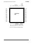
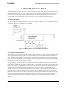

Table Of Contents
- About This Document
- 1 Introduction
- 2 Quick Start for the OEM Kit Users
- 3 Product Overview
- 4 IRIS OEM Reference Board
- 5 Power
- 6 Radios
- 7 Antennas
- 8 Flash Data Logger and Serial ID Chip
- 9 Atmega1281 Fuses
- 10 Sensor Boards & Expansion Connectors
- 11 USB Programming Pod
- 12 Appendix A. Warranty and Support Information

IRIS OEM Edition Hardware Reference Manual
4 IRIS OEM Reference Board
The IRIS OEM reference board is a carrier PCB with the same form factor and functionality as
the IRIS family product. It consists of a surface mount module consisting of a processor core
and a two-way radio, high density digital interface connector, RF coaxial antenna connector,
power supply connection, battery pack connection, power switch, and mounting holes.
4.1 Block Diagram
The block diagram for OEM reference board is provided in Figure 4-1. The detailed schematics
and Gerber files are provided in the CD-ROM.
Figure 4-1. Block diagram of the OEM Reference Board
4.2 Layout Considerations
The reference design requires specific support for the module. I/O pins used for communication
with peripherals will require pull-up resistors (10kΩ), such as the UART transmit and receive
pins. The RF out port must be connected to a 50 ohm trace to the antenna terminal. A ground
plane and proper impedance control must be observed for optimum function. No additional RF
filtering is necessary for the reference design.
A typical design should include a ground plane under the STAMP to provide a good transition
between the 50 ohm RF port and the mating board. Connecting the grounds on both sides of the
RF pad is strongly recommended. Using a trace that has almost the same width as the RF pin
will also help to minimize impedance mismatch as the RF connection transitions from the
module to the board. Provide a ground flood on the surface of the board from the RF ground
terminals to the antenna connector where possible, using regularly spaced vias to the ground
plane in the area of the copper flood. Provide a clearance region between the flood and the 50
ohm trace that is at least equal to the width of the trace. A good value for the trace width is 37
mils with a dielectric thickness of 20 mils between the trace and the ground plane for FR4
material.
Page 14 Doc. # 7430-0549-01 Rev. B