
Installation Manual
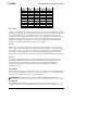
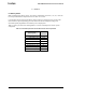
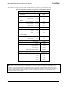


Table Of Contents
- About This Document
- 1 Introduction
- 2 Quick Start for the OEM Kit Users
- 3 Product Overview
- 4 IRIS OEM Reference Board
- 5 Power
- 6 Radios
- 7 Antennas
- 8 Flash Data Logger and Serial ID Chip
- 9 Atmega1281 Fuses
- 10 Sensor Boards & Expansion Connectors
- 11 USB Programming Pod
- 12 Appendix A. Warranty and Support Information

IRIS OEM Edition Hardware Reference Manual
Doc. # 7430-0549-01 Rev. B Page 21
single ended voltage inputs are reference to 0V (GND). The ADC ports are high impedance
inputs to the ADC, used for voltage sampling. The uppermost bits (ADC[4..7]) also support the
JTAG interface. The JTAG port can be enabled by choosing that option in the fuse bits for the
processor. Choosing the JTAG active option will cause approximately 50k ohms to be applied
from the ADC pin to VCC. This setting can affect the accuracy of ADC readings from weak
sources.
Table 4-5. JTAG Pin Definitions
PIN PORT
ADC4 TCK
ADC5 TMS
ADC6 TDO
ADC7 TDI
RSTN RSTN
The JTAG programming capability supports:
•
Flash programming and verifying
•
EEPROM programming and verifying
•
Fuse programming and verifying
•
Lock bit programming and verifying
4.5.7 GPIO
The remainder of the I/O pins is available as GPIO under processor configuration control. All
GPIO ports have true Read-Modify-Write functionality when used as general digital I/O ports.
This means that the direction of one port pin can be changed without unintentionally changing
the direction of any other pin with the SBI and CBI instructions. The same applies when
changing drive value (if configured as output) or enabling/disabling of pull-up resistors (if
configured as input). They can be left floating if not used, or can be set as inputs with a weak
pull-up, outputs set high, or outputs set low.