
Instruction manual


Operation Manual
M Series Power Amplifiers
page 16
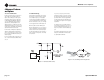
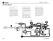
5 Principles of Operation
For the sake of simplicity, only channel one of
the amplifier is described.
Signal is presented to the M120 and M240
through one of three connectors when using
the standard input module. Each channel is
outfitted with a balanced XLR / phone jack, and
a barrier strip. These connectors are wired in
parallel, which allows daisy chaining when
needed. The signal is then converted from bal-
anced to unbalanced in the Balanced Input
Stage where it also receives RFI protection.
Signal then flows into the Variable Gain Stage
where the front panel level controls are allowed
to affect the gain.
Following this stage, the signal is put under the
control of a full-time compressor circuit com-
prised of a symmetrical window detector, a
buffer amplifier, and the gating op amp which
uses several small components to set the com-
pressor’s attack and decay characteristics. The
actual compressing is accomplished by an
opto-isolator which affects the gain in the sig-
nal path.
The signal next enters the main amplifier error
amp where it is mixed with a small portion of
the output signal in such a way as to control the
amplifier’s overall output performance.
Following the error amp is the LVA stage, which
is where the low-voltage referenced signal gets
translated to the output high-voltage rails. The
last voltage amplifier, in conjunction with a
bootstrapped current source, drives both pre-
drivers and the bias servo. The bias servo is
mounted in such a way as to translate the out-
put heatsink temperature into a controlled bias
current to prevent thermal runaway and hold
the amplifier’s notch distortion to a minimum.
The predrivers provide enough signal to acti-
vate the drivers, which together operate in the
class AB range. For the major output current
requirements, the drivers feed the various num-
bers of paralleled output transistors which
operate in a class B mode. This we call the Tri-
ple-Deep Darlington Output Stages.
TRANSLATOR LVA
BIAS
CURRENT
SOURCE
BALANCE
INPUT STAGE
VARIABLE
GAIN STAGE
ERROR
AMP
BALANCED
INPUTS
TO SIGNAL
PRESENCE
INDICATOR
COMPRESSOR
CONTROL
TO CLIP
INDICATOR
BUFFER
MUTE
DC PROTECT
LOGIC
TO
FAULT
CONNECTOR
–VCC
–VCC
+ HI-VOLTAGE
BOOTSTRAP
BIASBIASBIASBIASBIAS
TDVI
LIMITER
TRIPLE-DEEP
DARLINGTON
NPN POSITIVE
OUTPUT STAGE
TRIPLE-DEEP
DARLINGTON
NPN NEGATIVE
OUTPUT STAGE
PROPORTIONAL
SPEED
FAN
CONTROL
FAN
DC
PROTECT
HEATSINK
TEMPERATURE
OUTPUT
CONTROL
HEATSINK
TEMPERATURE
TRANSFORMER
TEMPERATURE
TO FAULT
INDICATOR
POWER
SUPPLY
+ VCC
+ 15V
– 15V
– VCC
TURN-ON
DELAY
+
OUTPUT
BOOTSTRAP
CIRCUIT
+ HI-VOLTAGE
BOOTSTRAP
Figure 5.1
M-Series Amplifier
Block Diagram
(Shown with Stan-
dard Input Module)