
Datasheet
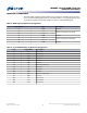
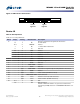
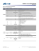
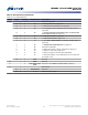
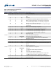

Table 5: Identify Device (Continued)
See Note 1 for setting definitions
Word Bit(s) Setting Default Value Description
59 15 F 1b 1 = The BLOCK ERASE EXT command is supported
14 F 1b 1 = The OVERWRITE EXT command is supported
13 F 1b 1 = The CRYPTO SCRAMBLE EXT command is supported
12 F 1b 1 = The sanitize feature set is supported
11–9 F 000b Reserved
8 V 1b 1 = Multiple sector settings are valid
7–0 V 00010000b xxh = Current setting for number of logical sectors that shall be
transferred per DRQ data block on READ/WRITE MULTIPLE com-
mands
60 – M(F) Varies by capacity Total number of user addressable logical sectors
62 – ( )X 0000h Obsolete
63 15–11 F 00000b Reserved
10 V 0b 1 = Multiword DMA mode 2 is selected
0 = Multiword DMA mode 2 is not selected
9 V 0b 1 = Multiword DMA mode 1 is selected
0 = Multiword DMA mode 1 is not selected
8 V 0b 1 = Multiword DMA mode 0 is selected
0 = Multiword DMA mode 0 is not selected
7–3 F 0000b Reserved
2 F 1b 1 = Multiword DMA mode 2 and below are supported
1 F 1b 1 = Multiword DMA mode 1 and below are supported
0 F 1b 1 = Multiword DMA mode 0 is supported
64 15–8 F 00h Reserved
7–0 F 03h PIO modes is supported
65 – F 0078h Minimum Multiword DMA transfer cycle time per word
Cycle time in nanoseconds
66 – F 0078h Manufacturer's recommended Multiword DMA transfer cycle
time
Cycle time in nanoseconds
67 – F 0078h Minimum PIO transfer cycle time without flow control
Cycle time in nanoseconds
68 – F 0078h Minimum PIO transfer cycle time with IORDY flow control
Cycle time in nanoseconds
M500DC 2.5-Inch NAND Flash SSD
Device ID
PDF: 09005aef854b6757
M500DC_2_5_disti.pdf - Rev. D 4/14 EN
8
Micron Technology, Inc. reserves the right to change products or specifications without notice.
© 2013 Micron Technology, Inc. All rights reserved.