
User's Guide

2015 Microchip Technology Inc. Advance Information DS00000A-page 9
RN2903
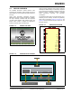
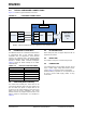
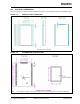
4.0 PHYSICAL DIMENSIONS
Figure 4-1 and Figure 4-2 illustrate the physical dimensions and the recommended PCB layout for the RN2903 module.
FIGURE 4-1: RN2903 PHYSICAL DIMENSIONS
FIGURE 4-2: RECOMMENDED PCB FOOTPRINT
Note: Host PCB top layer copper traces must have solder mask to avoid shorting test pins on the bottom of the module.