
Specifications


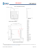


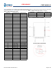


Table Of Contents
- CYBT-243053-02, EZ-BT™ Module
- General Description
- Benefits
- More Information
- Overview
- Pad Connection Interface
- Recommended Host PCB Layout
- Module Connections
- Connections and Optional External Components
- Critical Components List
- Antenna Design
- Bluetooth Baseband Core
- Power Management Unit
- Integrated Radio Transceiver
- Microcontroller Unit
- Peripherals and Communication Interfaces
- Electrical Characteristics
- Chipset RF Specifications
- Timing and AC Characteristics
- Environmental Specifications
- Regulatory Information
- Packaging
- Ordering Information
- Acronyms
- Document Conventions
- Document History Page
- Sales, Solutions, and Legal Information

Document Number: 002-28015 Rev. ** Page 6 of 42
PRELIMINARY
CYBT-243053-02
Figure 3. Solder Pad Dimensions (Seen from Bottom)
To maximize RF performance, the host layout should follow these recommendations:
1. Antenna Area Keepout: The host board directly below the antenna area of the Cypress module (see Figure 2 on page 5) must
contain no ground or signal traces. This keep out area requirement applies to all layers of the host board.
2. Module Placement: The ideal placement of the Cypress Bluetooth module is in a corner of the host board with the PCB antenna
located at the far corner. This placement minimizes the additional recommended keep out area stated in item 3 below. Refer to
AN96841 for module placement best practices.
3. Optional Keepout: To maximize RF performance, the area immediately around the Cypress Bluetooth module PCB antenna may
contain an additional keep out area, where there are no grounding or signal traces. The keep out area applies to all layers of the
host board. The recommended dimensions of the host PCB keep out area are shown in Figure 4 (dimensions are in mm).
Figure 4. Optional Additional Host PCB Keep Out Area Around the CYBT-243053-02 PCB Antenna
Pad Connection Interface
As shown in the bottom view of
Figure 2 on page 5, the CYBT-243053-02 has 35 connections to a host board via solder pads (SP).
Table
2
and
Figure
3
detail the solder pad length, width, and pitch dimensions of the CYBT-243053-02 module.
Table 2. Connection Description
Name Connections Connection Type Pad Length Dimension Pad Width Dimension Pad Pitch
0.90 mm0.61 mm1.02 mmSolder Pad35SP
Solder Pad Connections (Seen from Bottom)
Optional Host PCB Keep Out
Area Around PCB Antenna
(Seen from Bottom)