
User's Manual
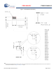
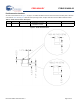
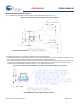
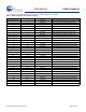
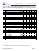

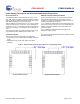
Table Of Contents
- General Description
- Contents
- Overview
- Pad Connection Interface
- Recommended Host PCB Layout
- Power Supply Connections and Recommended External Components
- Electrical Specification
- Environmental Specifications
- Regulatory Information
- Ordering Information
- Acronyms
- Document Conventions
- Errata
- Document History Page
- Sales, Solutions, and Legal Information

PRELIMINARY
CYBLE-214009-00
Document Number: 002-09714 Rev. ** Page 8 of 40
Table 4 and Tabl e 5 detail the solder pad connection definitions and available functions for each connection pad. Table 4 lists the
solder pads on CYBLE-214009-00, the BLE device port-pin, and denotes whether the digital function shown is available for each
solder pad. Table 5 denotes whether the analog function shown is available for each solder pad. Each connection is configurable for
a single option shown with a
3.
Table 4. Digital Peripheral Capabilities
Pad
Number
Device
Port Pin
UART SPI I
2
C TCPWM
[2]
Cap-
Sense
WCO
Out
ECO
OUT
LCD SWD GPIO
1GND
[3]
Ground Connection
2P1.1
3(SCB1_SS1) 3(TCPWM0) 333
3P1.0 3(TCPWM0) 333
4P1.53(SCB0_TX) 3(SCB0_MISO) 3(SCB0_SCL) 3(TCPWM2) 333
5P0.13(SCB1_TX) 3(SCB1_MISO) 3(SCB1_SCL) 3(TCPWM0) 333
6P0.73(SCB0_CTS) 3(SCB0_SCLK) 3(TCPWM2) 33
3
(SWDCLK)
3
7 VDD Digital Power Supply Input (1.71 to 5.5V)
8P1.4
3(SCB0_RX) 3(SCB0_MOSI) 3(SCB0_SDA) 3(TCPWM2) 333
9P0.43(SCB0_RX) 3(SCB0_MOSI) 3(SCB0_SDA) 3(TCPWM1) 333 3
10 P0.5 3(SCB0_TX) 3(SCB0_MISO) 3(SCB0_SCL) 3(TCPWM1) 333
11 P0.6 3(SCB0_RTS) 3(SCB0_SS0)
3(TCPWM2) 333
(SWDIO)
3
12 P1.2 3(SCB1_SS2) 3(TCPWM1) 333
13 V
DDR
Radio Power Supply (1.9V to 5.5V)
14 P2.6
333
15 P1.3 3(SCB1_SS3) 3(TCPWM1) 333
16 P3.0 3(SCB0_RX) 3(SCB0_SDA) 3(TCPWM0) 333
17 P2.1 3(SCB0_SS2) 333
18 P2.2 3(SCB0_SS3) 333
19 P2.3 33 3 3
20 VDDA Analog Power Supply Input (1.71 to 5.5V)
21 P3.4
3(SCB1_RX) 3(SCB1_SDA) 3(TCPWM2) 333
22 P3.1 3(SCB0_TX) 3(SCB0_SCL) 3(TCPWM0) 333
23 P3.7 3(SCB1_CTS) 3(TCPWM3) 33 3 3
24 P3.5 3(SCB1_TX) 3(SCB1_SCL) 3(TCPWM2) 333
25 P3.3 3(SCB0_CTS) 3(TCPWM1) 333
26 VREF Reference Voltage Input
27 P3.2
3(SCB0_RTS) 3(TCPWM1) 333
28 P3.6 3(SCB1_RTS) 3(TCPWM3) 333
29 XRES External Reset Hardware Connection Input
30 P2.4
333
31 P2.5 333
32 GND Ground Connection
Notes
2. TCPWM stands for timer, counter, and PWM. If supported, the pad can be configured to any of these peripheral functions.
3. The main board needs to connect both GND connections (Pad 1 and Pad 32) on the module to the common ground of the system.