
User's Manual


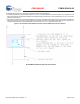

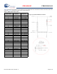
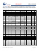
Table Of Contents
- General Description
- More Information
- Contents
- Overview
- Pad Connection Interface
- Recommended Host PCB Layout
- Power Supply Connections and Recommended External Components
- Electrical Specifications
- Environmental Specifications
- Regulatory Information
- Packaging
- Ordering Information
- Acronyms
- Document Conventions
- Document History Page
- Sales, Solutions, and Legal Information

PRELIMINARY
CYBLE-224110-00
Document Number: 002-11264 Rev. *A Page 10 of 43
Table 4 and Table 5 detail the solder pad connection definitions and available functions for each connection pad. Table 5 lists the
solder pads on CYBLE-224110-00, the BLE device port-pin, and denotes whether the digital function shown is available for each
solder pad. Table 5 denotes whether the analog function shown is available for each solder pad. Each connection is configurable for
a single option shown with a 3.
Table 4. Digital Peripheral Capabilities
Pad
Number
Device
Port Pin
UART SPI I
2
C TCPWM
[2]
Cap
Sense
WCO
Out
ECO
OUT
LCD SWD GPIO
1GND
[3]
Ground Connection
2 XRES External Reset Hardware Connection Input
3P1.5
3(SCB0_TX) 3(SCB0_MISO) 3(SCB0_SCL) 3(TCPWM2_N)
333
4P1.1 3(SCB1_SS1) 3(TCPWM0_N)
333
5P1.0 3(TCPWM0_P)
333
6P0.13(SCB1_TX) 3(SCB1_MISO) 3(SCB1_SCL) 3(TCPWM0_N)
333
7P0.43(SCB0_RX) 3(SCB0_MOSI) 3(SCB0_SDA) 3(TCPWM1_P)
333 3
8P0.53(SCB0_TX) 3(SCB0_MISO) 3(SCB0_SCL) 3(TCPWM1_N)
333
9P0.73(SCB0_CTS) 3(SCB0_SCLK) 3(TCPWM2_N)
33
3
(SWDCLK)
3
10 P1.3 3(SCB1_SS3) 3(TCPWM1_N)
333
11 V
DDR
Radio Power Supply (2.0V to 3.6V)
12 P0.6
3(SCB0_RTS) 3(SCB0_SS0)
3(TCPWM2_P) 33
3
(SWDIO)
3
13 P1.2 3(SCB1_SS2) 3(TCPWM1_P)
333
14 V
DD
Digital Power Supply Input (1.71 to 5.5V)
15 P1.4 3(SCB0_RX) 3(SCB0_MOSI) 3(SCB0_SDA) 3(TCPWM2_P)
333
16 P2.1 3(SCB0_SS2)
333
17 V
DDA
Analog Power Supply Input (1.71 to 5.5V)
18 P2.2 3(SCB0_SS3)
333
19 P2.6
333
20 P3.0 3(SCB0_RX) 3(SCB0_SDA) 3(TCPWM0_P)
333
21 P2.3
33 3 3
22 V
REF
Reference Voltage Input
23 P3.4 3(SCB1_RX) 3(SCB1_SDA) 3(TCPWM2_P)
333
24 P3.5 3(SCB1_TX) 3(SCB1_SCL) 3(TCPWM2_N)
333
25 P3.7 3(SCB1_CTS) 3(TCPWM3_N)
33 3 3
26 P3.1 3(SCB0_TX) 3(SCB0_SCL) 3(TCPWM0_N)
333
27 P3.6 3(SCB1_RTS) 3(TCPWM3_P)
333
28 P2.5
333
29 P5.0 3(SCB1_RX) 3(SCB1_SS0) 3(SCB1_SDA) 3(TCPWM3_P)
333
30 P5.1 3(SCB1_TX) 3(SCB1_SCLK) 3(SCB1_SCL) 3(TCPWM3_N)
333 3
31 P2.4
333
32 GND
[3]
Ground Connection