ENGLISH Altera Application Solutions Guide Book ® December 2011 Prepared by Group Companies
Altera® Application Solutions Guide Book – December 2011 2
Index INTRODUCTION TO MACNICA GROUP ........................................................................ 5 About Macnica Group................................................................................................................................5 Group Structure and Subsidiaries ...........................................................................................................6 ALTERA® APPLICATION SOLUTIONS GUIDE BOOK – NOVEMBER 2011 ................. 7 VIDEO SYSTEM SOLUTIONS .........
Software Development Tools ...............................................................................................................36 Nios II Embedded Design Suite ..........................................................................................................36 Embedded Software Partners .............................................................................................................36 Hardware Development Tools ..................................................................
Introduction to Macnica Group Altima Corp., Elsena, Inc., Cytech Technology Ltd. and Galaxy Far East Corp. are the Macnica Group companies with the common supplier - Altera Corporation - in their line card and the common corporate culture aiming at providing the customers with high level of technical solutions in addition to selling the products.
and technical insight. Macnica will find things existed nowhere and bring them here for you. Macnica Group keeps going, with challenges. “NOWHERE, but HERE.” Macnica Group Facts Established October 30, 1972 President & CEO Kiyoshi Nakashima Paid-in Capital JPY 11,194,268,000 (as of March 31, 2011) Publicly traded at The 1st Division of Tokyo Stock Exchange (Symbol: 7631.t) Revenue FY06 FY07 FY08 FY09 FY10 JPY 163.6 Billion JPY 154.1 Billion JPY 131.5 Billion JPY 149.2 Billion JPY 188.
Altera® Application Solutions Guide Book – November 2011 Altima Corp., Elsena, Inc., Cytech Technology Ltd. and Galaxy Far East Corp. are the Macnica Group companies with the common supplier Altera Corporation in their line card and the common corporate culture aiming at providing the customers with high level of technical solutions in addition to selling the products.
Video System Solutions Your Video System Design Starts Here … Before you start your next video system design, check out the largest, most comprehensive collection of video solutions in the FPGA industry.
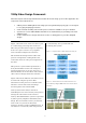
1080p Video Design Framework Altera developed a video design framework that enables the fastest design cycle for video application.
Finally, the entire video design framework really comes together in the form of an HD reference design that showcases the actual video processing common to many applications. Altera developed several reference designs that were driven by actual customer demand for scaling, mixing, and processing HD video streams over serial digital interfaces (SDI). Figure 4 shows one of the reference designs that processes 1080p quality video. This design was built using the Altera video design framework.
2.
3. Altera's partner Bitec has developed multiple reference designs that work with Cyclone III Video Dev Kit. Visit Altera web site to get designs that showcase color space conversion, Picture-in-Picture, 4-channel video compositing and even a 1080p H.264 encoder design. 4. Altera's partner Microtronix has also developed a portfolio of video reference designs that are available with their Stratix III Broadcast IP Dev Kit and with their Cyclone III ViClaro Video Dev Kit.
Video Development Board Solutions Audio Video Development Kit, Stratix IV GX Edition Altera Corporation The Audio Video Development Kit, Stratix IV GX Edition, delivers a complete video and image processing development environment for design engineers.
Cyclone III FPGA Development Kit Altera Corporation Altera's Cyclone III FPGA Development Kit combines Embedded USB-Blaster™ circuitry (includes Display the largest density low-cost, low-power FPGA an Altera MAX II CPLD) allowing download of available with a robust set of memories and user FPGA configuration files via the flash device or interfaces.
Board Solutions from Third Party Board Partners Daughter Cards USB 2.0 + Gigabit Ethernet SD/HD-SDI 2 CH high speed AD/DA 105M Dual 100M Industrial Ethernet Audio / Video HSMA SMA IO expandable FE-4CGX150 Hangzhou Free Electron Co. Ltd Altera Cyclone IV GX FPGA development platform Features • FPGA:EP4CGX150DF27C8 • Config: support FPP, support 4 different config • Sync SSRAM: CY7C1360C-200AXC • DDR2 SD RAM: 32bit, 128M Byte • SFP: 1 channel, support as fast as 3.
Broadcast Video Card DVI Input/Output Card Bitec Ltd. Cyclone III SDALTEVK Kit Bitec Ltd. Bitec Ltd. Develop profesional video fpga based systems using Two channel Dual-Link DVI output board for Altera Features the Bitec BVDC. FPGA development kits with HSMC expansion port.
Quad Link LVDS Interface HSMC Gigabit Ethernet PHY / HDMI DVI Receiver / Transmitter HSMC Board Transmitter HSMC Board Board Microtronix Datacom Ltd. Microtronix Datacom Ltd. Microtronix Datacom Ltd.
Altera DE4 Development and 5 Mega Pixel Digital Camera Education Board Package Terasic Technologies SDI-HSMC Card Terasic Technologies Terasic Technologies Features Features The Transceiver Serial Digital Interface (SDI) HSMC • Stratix IV GX EP4SGX230/EP4SGX530 with • Reference design with Verilog source code board provides a hardware platform for developing • A User Manual with Live Demo examples video broadcasting systems. It is intended to be used • PCIe 2.
High Speed External Memory Interface Solutions Altera's complete memory interface design solutions address today's high-speed memory interface challenges such as memory controller, I/O design, and board-level signal integrity issues. Altera's solutions include advanced device architectures, customizable MegaCore® functions, Quartus® II design software, reference designs, demonstration boards, and simulation models, accompanied by a rich set of technical documentation.
DRAM Device Overview DRAM devices are volatile memories offering a lower cost per bit than SRAM devices. A compact memory cell consisting of a capacitor and a transistor makes this possible over the six-transistor cell used in SRAM. However, the capacitor will discharge, causing the memory cell to lose its state, which means that DRAM memory needs to be refreshed periodically. Generally, you would choose SRAM devices for applications where latency or low interface complexity is important.
RLDRAM II RLDRAM II is the second generation of RLDRAM. It is a development of DDR SDRAM, designed to address the low latency requirements of certain applications, such as packet buffers in high-performance line cards. RLDRAM II has a high-performance DDR data bus and offers a non-multiplexed address bus, reducing the number of clock cycles to initiate read or write applications. A banked architecture also reduces access time.
developed the QDR architecture. QDR is designed to meet the high-performance needs of high-speed networking applications. ZBT SRAM Devices ZBT SRAM is a synchronous burst SRAM with a simplified interface that provides higher bandwidth and efficient bus utilization by eliminating turnaround cycles and idle cycles between read and write operations. IDT, Micron, and Motorola jointly developed the ZBT SRAM architecture, which is optimized for networking and telecommunications applications.
External Memory Interface Board Solutions Stratix IV E FPGA Development Kit Altera Corporation The Altera Stratix IV GX FPGA Development Kit Features • Two HSMC connectors delivers a complete system-level design environment • Altera Stratix IV GX EP4SGX230KF40C2N • HDMI video output 3G SDI video input and output that includes both the hardware and software needed • On-board clock oscillators • Power & Temperature measurement circuitries to immediately begin developing FPGA designs.
Board Solutions from Third Party Board Partners ALL-IN-ONE Base Board B-11 (Stratix III Edition) Accverinos Co.,Ltd. CycloneIII SOPC board Hangzhou Free Electron Co. Ltd Features This board offer Ethernet, DDR2 interface, enough • EP3SL340F1517 or EP3SL200F1517 (-2 or -3) test port and expend IO. It is suitable for SOPC • DDR2 DIMM system design and small/middle density IP/ASIC • DVI I/O Support: 1 each of input and output port using TI TFP403 & 410 chips. verification.
High Speed Interface Solutions Transceiver Portfolio Altera is a pioneer and leader in integrating transceivers into FPGAs. In 2001, we introduced our first FPGA family with integrated transceivers. Since then, we've introduced many innovations to make transceivers run faster, operate more reliably, and support emerging protocols with each generation of FPGAs and ASICs. With a top-notch, in-house transceiver design team, we're equipped to continue tailoring transceivers for specific applications.
design software, a common set of IP cores, sophisticated signal integrity tools, and a variety of supporting reference designs and design examples. Learn the software once, then extend your skills across multiple design platforms.
Stratix® Series FPGAs Protocol V GX/GS V GT IEEE 802.3ba 100G HardCopy ASICs IV GX IV GT V GX - Arria® Series FPGAs Cyclone® Series FPGAs IV GX II GX IV GX - - - - - Interlaken Interlaken (10G) - - - - OTU-2 (G.
Plug & Play Signal Integrity Available in Stratix® and Arria® series FPGAs and HardCopy® ASICs with integrated multi-gigabit transceivers, Plug & Play Signal Integrity lets you change the position of backplane cards on the fly while eliminating the painstaking process of manually reconfiguring your backplane equalization settings With this capability, you can design systems with truly universal cards that plug into multiple card positions in system backplanes (as shown in this picture in the right.
High Speed Interface Board Solutions Transceiver Signal Integrity Development Kit, Stratix IV GT Edition Altera Corporation Altera's Transceiver Signal Integrity Development • DIP and push-button switches • RJ-45 jack and 10/100/1000Base-T Ethernet PHY Kit, Stratix IV GT Edition enables a thorough • LEDs • Backplane drive capability at 6.
Arria II GX FPGA Development Kit Altera Corporation The Altera Arria II GX FPGA Development Kit Features delivers a complete system-level design environment • Arria II GX EP2AGX125EF35 FPGA Programmable oscillator, default frequency that includes both the hardware and software needed • On-board ports 125 MHz Programmable oscillator, default frequency to immediately begin developing FPGA designs.
Board Solutions from Third Party Board Partners 3FAD/D4-AMC 3FDJ/D4-AMC BittWare, Inc. 3FAD/S4-3U-VPX BittWare, Inc. BittWare, Inc.
Back Altera Stratix IV GX/GT PCI / Front HTG-FMC-CX4-SATA-SMA Back / Front HTG-FMC-2CX4 Express Gen 2 / USB 3.
Embedded System Design Solution Why Use FPGAs in Embedded Designs? Altera’s powerful development tools let you create custom systems on a programmable chip, making FPGAs the platform of choice. When you think embedded, think FPGAs, think Altera. Here’s why: • Increase productivity Whether you are a hardware designer or software developer, we have tools to provide you with unprecedented time and cost savings.
Step 1: Get the Design Software There are several ways to get the Nios II processor and Nios II EDS development tools: Web download—All the software tools you need to start development are available for immediate download: the Quartus® II design software, the Nios IDE, and the SOPC Builder system development software. Download software from the Altera site.
Step 3: Purchase Licensing Purchase a license for the Nios II processor IP core and related products. Nios II IP Core and Related Products Nios II Processor IP Get a license file for the Nios II processor, non-time-limited use, by purchasing a Nios II development kit or the stand-alone Nios II processor core license (ordering code: IP-NIOS). Both fixed and floating licenses are available. To obtain a license file, contact your local Altera representative or Altera Tools Support.
Software Development Tools Altera, along with its embedded software partners, offers a range of powerful tools for your software development needs. Nios II Embedded Design Suite The Nios® II Embedded Design Suite (EDS) is a collection of components and tools used to develop embedded software for the Nios II processor, including Nios II Software Build Tools for Eclipse based on the familiar Eclipse development environment. The Nios II IDE is also included to provide support for legacy designs.
Quartus II FPGA System Design Tool Altera’s Quartus® II software leads the industry as the most comprehensive environment available for FPGA designs, providing unmatched performance delivery, efficiency, and ease-of-use. SOPC Builder System-Level Integration Tool SOPC Builder eliminates manual system integration tasks and allows you to focus on custom user logic design to differentiate your system. All versions of the Altera® Quartus II design software include the SOPC Builder system generation tool.
Embedded Systems Board Solutions Altera Embedded System Development Kit, Cyclone III Edition Altera Corporation The Altera Embedded Systems Development Kit, A Cyclone III FPGA-based board with • U-boot files Cyclone III Edition is a complete development high-speed mezzanine card (HSMC) connectors • Out-Of-Box Experience platform for prototyping embedded systems on to interface to a wide range of daughtercards • This board is, in itself, an embedded system.
MAX II Development Kit Altera Corporation The MAX II Development Kit enables you to evaluate • Power measuring circuit—Allows users to measure the MAX II CPLD feature set or begin prototyping the stand-by and nominal power consumed by the your own design.
Cyclone III USB3.0 Board ALTIMA Corp. Altima’s “Cyclone III USB 3.0 Bard” is an evaluation board for USB 3.0 interface by combining FPGA and USB 3.0 PHY devices. The user of this board can attain higher flexibility in setting up different evaluation configurations in USB 3.0 controller functions implemented in Cyclone III low cost FPGA. Also, the user can utilize HSMC connector to bridge to various interface standards at the same time. • Texas Instruments (TI) - TSUB1310 USB 3.
Altera FPGA + Cypress PSoC EVK Cytech Technology, Ltd. Cyctech’s “Altera FPGA + Cypress PSoC EVK” is a • PSoC + FPGA + SRAM integrated starter kit for Altera Cyclone III FPGA and Cypress • CapSense GPIOs pulled out • Documentation and support deliverables PSoC1. The kit provides a set of low cost, easy and Three CapSense Buttons Schematics convenient tool for learning FPGA and PSoC and for One CapSense Slider PCB data R&D using FPGA and PSoC.
Galaxy MAX II Starter Kit Galaxy Far East Corp. The MAXII Starter kit provide a tool of enter Features FPGA/CPLD world , Anybody can use Altera free web • Altera edition software Quartus II study FPGA/CPLD design MAX II CPLD EPM1270T144C5 technique more easier. The Altera’s MAXII family is a • 4 Digitals seven segment LED Display high volume low cost product, it provide bigger logic • 8 Bits DIP Switch capacity and lower power consumption than tradition • 4 Push Button Switchs CPLD.
ACM-022 - Altera Cyclone III F780 FPGA board ACM-202 - Altera Cyclone III F780 FPGA board Humandata Ltd. Altera DE2-115 Development and Education Board Terasic Technologies Humandata Ltd.
ASIC Prototyping Why use FPGAs for ASIC prototyping? In the modern ASIC design flow, the use of logic simulator software had been a relevant choice of technique for ASIC designers for long time as the older process ASIC had limited size of the designs. Also, the lower cost of the mask iterations allowed the designers to spin the design several times per project.
Parallel verification The FPGA prototyping method allows the hardware design and software verification simultaneously (hardware-software co-design). The verification period can be dramatically reduced by verifying software by functionality on multiple prototype boards in parallel. The figure shows how the parallel verification improves the verification process in the design flow.
Frequently Asked Questions Following is the list of questions and answers for ASIC designers without experience of using FPGA. the simulation speed is usually very slow as several MHz and the total time needed for FPGA prototyping is much faster. Q1. It is more realistic to use the high level verification for algorithm and FPGA prototyping for system verification.
process of specification writing and logic simulation. A5. Unfortunately, you cannot do the timing verification on the FPGA prototype as the timing for ASIC and FPGA are different. However, doing the functional verification on the FPGA board is a very effective way to reduce reiteration of ASIC designs as the most common reason for ASIC re-spin is the functional errors.
ASIC Prototyping Board Solutions Stratix IV ASIC Prototyping Board EK4SEH40 Galaxy Far East Corp. Altera Stratix IV-E FBGA1517 FPGA Prototyping • Oscillator Socket Altera Stratix IV-E FBGA1517 FPGA Prototyping Module • Provide 757 In/Out Pin (With I/O Protection buffer) Module The module use Altera Stratix IV-E family FPGA • 1 Mictor Connector The module use Altera Stratix IV-E family FPGA with FBGA (Fine Line Ball Array) 1517 pin package • Power System For Altera device (1.1V/3.0V/2.
S4 TAI Logic Module for SOC prototype DE3 Development System S2C Inc. Terasic Technologies This platform used 2 pcs Altera StratixIV (EP4SE530 Features /EP4SE820) FPGA, can verify 16.4M ASIC gate • Stratix III 3SL150, 260 or 340 design.
Contact Information For product details and inquiries, please contact your local Macnica Group companies with Altera franchise. Japan ALTIMA Corp. Headquarters: Shin-Yokohama 1-5-5 Shin-Yokohama, Kouhoku-ku, Yokohama, 222-8563 Japan Tel: +81-45-476-2155 Fax: +81-45-476-2156 http://www.altima.co.jp Sales Offices Osaka Tel: +81-6-6397-1053 Fax: +81-6-6397-1054 ELSENA, Inc.
© 2011 Altima Corp., Elsena, Inc., Cytech Technology, Ltd. & Galaxy Far East Corp.